74LV04 All information provided in this document is subject to legal disclaimers. © NXP Semiconductors N.V. 2015. All rights reserved.
Product data sheet Rev. 4 — 8 December 2015 6 of 15
NXP Semiconductors
74LV04
Hex inverter
10. Dynamic characteristics
[1] All typical values are measured at T
amb
=25C.
[2] t
pd
is the same as t
PLH
and t
PHL
.
[3] Typical values are measured at nominal supply voltage (V
CC
= 3.3 V).
[4] C
PD
is used to determine the dynamic power dissipation (P
D
in W).
P
D
=C
PD
V
CC
2
f
i
N+(C
L
V
CC
2
f
o
) where:
f
i
= input frequency in MHz, f
o
= output frequency in MHz
C
L
= output load capacitance in pF
V
CC
= supply voltage in V
N = number of inputs switching
(C
L
V
CC
2
f
o
) = sum of the outputs.
Table 7. Dynamic characteristics
GND = 0 V; For test circuit see Figure 7.
Symbol Parameter Conditions 40 C to +85 C 40 C to +125 C Unit
Min Typ
[1]
Max Min Max
t
pd
propagation delay nA to nY; see Figure 6
[2]
V
CC
= 1.2 V - 40 - - - ns
V
CC
= 2.0 V - 14 20 - 25 ns
V
CC
= 2.7 V - 10 15 - 19 ns
V
CC
= 3.0 V to 3.6 V; C
L
=15pF
[3]
-6- - -ns
V
CC
= 3.0 V to 3.6 V
[3]
-812- 15ns
V
CC
= 4.5 V to 5.5 V - - 9 - 11 ns
C
PD
power dissipation
capacitance
C
L
=50pF; f
i
= 1 MHz;
V
I
=GNDtoV
CC
[4]
-21- - -pF
74LV04 All information provided in this document is subject to legal disclaimers. © NXP Semiconductors N.V. 2015. All rights reserved.
Product data sheet Rev. 4 — 8 December 2015 7 of 15
NXP Semiconductors
74LV04
Hex inverter
11. Waveforms
Measurement points are given in Table 8.
V
OL
and V
OH
are typical voltage output levels that occur with the output load.
Fig 6. The input (nA) to output (nY) propagation delays
PQD
W
3+/
W
3/+
9
0
9
0
9
0
9
0
Q$LQSXW
Q<RXWSXW
*1'
9
,
9
2+
9
2/
Table 8. Measurement points
Supply voltage Input Output
V
CC
V
M
V
M
< 2.7 V 0.5V
CC
0.5V
CC
2.7 V to 3.6 V 1.5 V 1.5 V
4.5 V 0.5V
CC
0.5V
CC
Test data is given in Table 9.
Definitions test circuit:
R
T
= Termination resistance should be equal to output impedance Z
o
of the pulse generator.
R
L
= Load resistance.
C
L
= Load capacitance including jig and probe capacitance.
Fig 7. Test circuit for measuring switching times
9
&&
9
,
9
2
DDD
'87
&
/
S)
5
7
5
/
Nȍ
38/6(
*(1(5$725
Table 9. Test data
Supply voltage Input
V
CC
V
I
t
r
, t
f
< 2.7 V V
CC
2.5 ns
2.7 V to 3.6 V 2.7 V 2.5 ns
4.5 V V
CC
2.5 ns
74LV04 All information provided in this document is subject to legal disclaimers. © NXP Semiconductors N.V. 2015. All rights reserved.
Product data sheet Rev. 4 — 8 December 2015 8 of 15
NXP Semiconductors
74LV04
Hex inverter
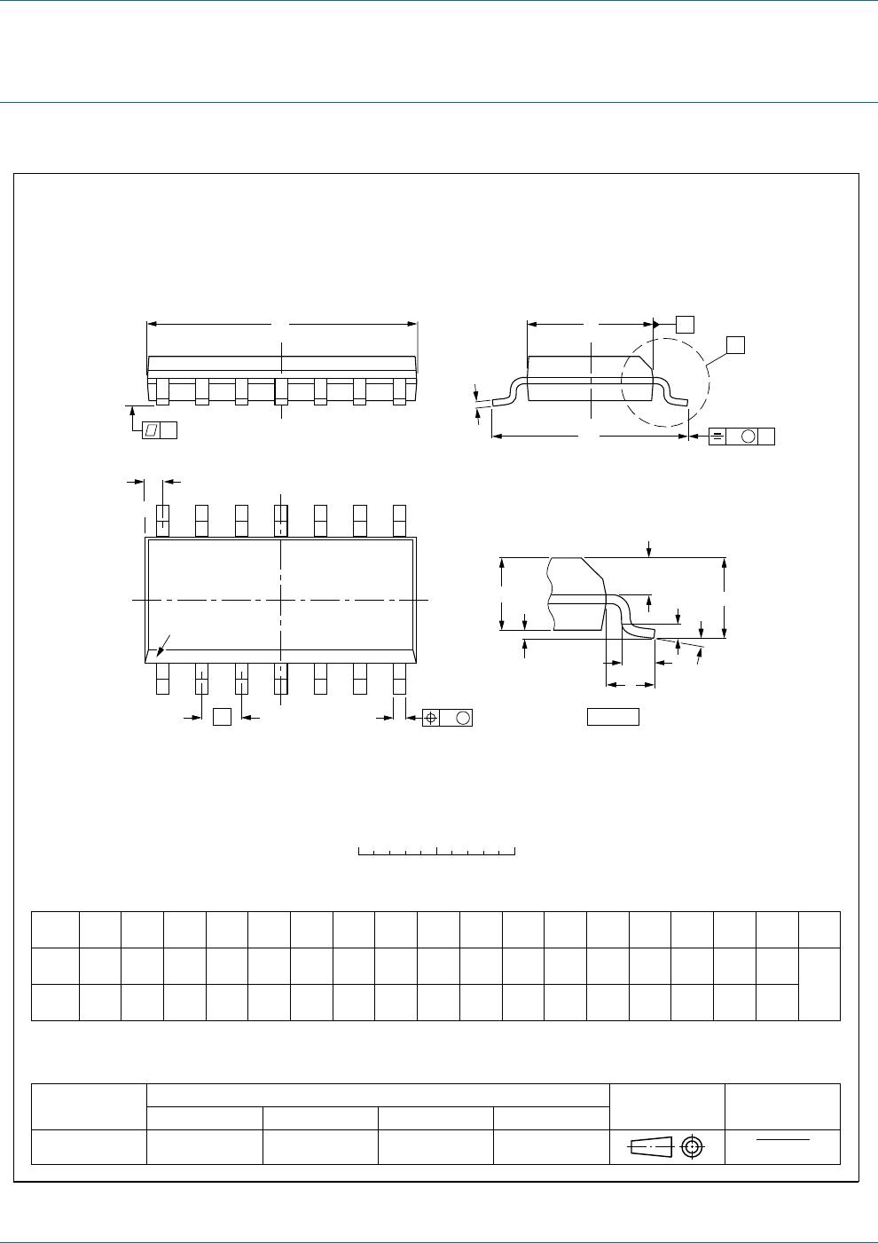
12. Package outline
Fig 8. Package outline SOT108-1 (SO14)
81,7
$
PD[
$

$

$

E
S
F '

(


H +
(
/ /
S
4 =\ZY ș
5()(5(1&(6
287/,1(
9(56,21
(8523($1
352-(&7,21
,668('$7(
,(& -('(& -(,7$
PP
LQFKHV























R
R
 
',0(16,216LQFKGLPHQVLRQVDUHGHULYHGIURPWKHRULJLQDOPPGLPHQVLRQV
1RWH
3ODVWLFRUPHWDOSURWUXVLRQVRIPPLQFKPD[LPXPSHUVLGHDUHQRWLQFOXGHG


627
;
Z 0
ș
$
$

$

E
S
'
+
(
/
S
4
GHWDLO;
(
=
H
F
/
Y 0
$
$

$




\
( 06
SLQLQGH[

























 




  PP
VFDOH
62SODVWLFVPDOORXWOLQHSDFNDJHOHDGVERG\ZLGWKPP
627

74LV04PW,118

Mfr. #:
Manufacturer:
Nexperia
Description:
Inverters HEX INVERTER 3-VOLT
Lifecycle:
New from this manufacturer.
Delivery:
DHL FedEx Ups TNT EMS
Payment:
T/T Paypal Visa MoneyGram Western Union