XC2C128 CoolRunner-II CPLD
DS093 (v3.2) March 8, 2007 www.xilinx.com 7
Product Specification
R
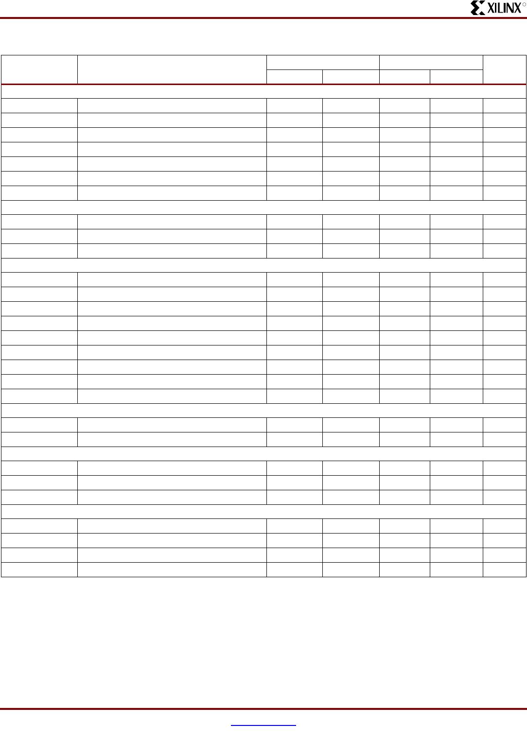
AC Electrical Characteristics Over Recommended Operating Conditions
Symbol Parameter
-6 -7
UnitsMin. Max. Min. Max.
T
PD1
Propagation delay single p-term - 5.7 - 7.0 ns
T
PD2
Propagation delay OR array - 6.0 - 7.5 ns
T
SUD
Direct input register set-up time 3.6 - 4.6 - ns
T
SU1
Setup time fast (single p-term) 2.4 - 3.0 - ns
T
SU2
Setup time (OR array) 2.7 - 3.5 - ns
T
HD
Direct input register hold time 0.0 - 0.0 - ns
T
H
Hold time (Or array or p-term) 0.0 - 0.0 - ns
T
CO
Clock to output - 4.2 - 5.4 ns
F
TOGGLE
(1)
Internal toggle rate - 450 - 300 MHz
F
SYSTEM1
(2)
Maximum system frequency - 244 - 152 MHz
F
SYSTEM2
(2)
Maximum system frequency - 227 - 141 MHz
F
EXT1
(3)
Maximum external frequency - 152 - 119 MHz
F
EXT2
(3)
Maximum external frequency - 145 - 112 MHz
T
PSUD
Direct input register p-term clock setup time 2.5 - 3.1 - ns
T
PSU1
P-term clock setup time (single p-term) 1.3 - 1.5 - ns
T
PSU2
P-term clock setup time (OR array) 1.6 - 2.0 - ns
T
PHD
Direct input register p-term clock hold time 0.2 - 0.2 - ns
T
PH
P-term clock hold 0.7 - 1.0 - ns
T
PCO
P-term clock to output - 5.9 - 7.3 ns
T
OE
/T
OD
Global OE to output enable/disable - 5.9 - 7.5 ns
T
POE
/T
POD
P-term OE to output enable/disable - 7.0 - 8.5 ns
T
MOE
/T
MOD
Macrocell driven OE to output enable/disable - 7.7 - 9.9 ns
T
PAO
P-term set/reset to output valid - 6.6 - 8.1 ns
T
AO
Global set/reset to output valid - 5.0 - 7.6 ns
T
SUEC
Register clock enable setup time 3.1 - 3.5 - ns
T
HEC
Register clock enable hold time 0.0 - 0.0 - ns
T
CW
Global clock pulse width High or Low 1.1 - 1.6 - ns
T
APRPW
Asynchronous preset/reset pulse width (High or Low) 6.0 - 7.5 - ns
T
PCW
P-term pulse width High or Low 6.0 - 7.5 - ns
T
DGSU
Set-up before DataGATE latch assertion 0.0 - 0.0 - ns
T
DGH
Hold to DataGATE latch assertion 4.0 - 6.0 - ns
T
DGR
DataGATE recovery to new data - 8.2 - 9.0 ns
T
DGW
DataGATE low pulse width 3.0 - 4.0 - ns
T
CDRSU
CDRST setup time before falling edge GCLK2 1.3 - 2.0 - ns
T
CDRH
Hold time CDRST after falling edge GCLK2 0.0 - 0.0 - ns
T
CONFIG
(4)
Configuration time - 350 - 350 us
Notes:
1. F
TOGGLE
is the maximum clock frequency to which a T flip-flop can reliably toggle (see the CoolRunner-II family data sheet).
2. F
SYSTEM1
is the internal operating frequency for a device with 16-bit resetable binary counter through one p-term per macrocell while
F
SYSTEM2
is through the OR array (one counter per function block).
3. F
EXT1
(1/T
SU1
+T
CO
) is the maximum external frequency using one p-term while F
EXT2
is through the OR array.
4. Typical configuration current during
T
CONFIG
is 10 mA.