MCP9501/2/3/4
DS22268A-page 6 © 2011 Microchip Technology Inc.
3.0 PIN DESCRIPTIONS
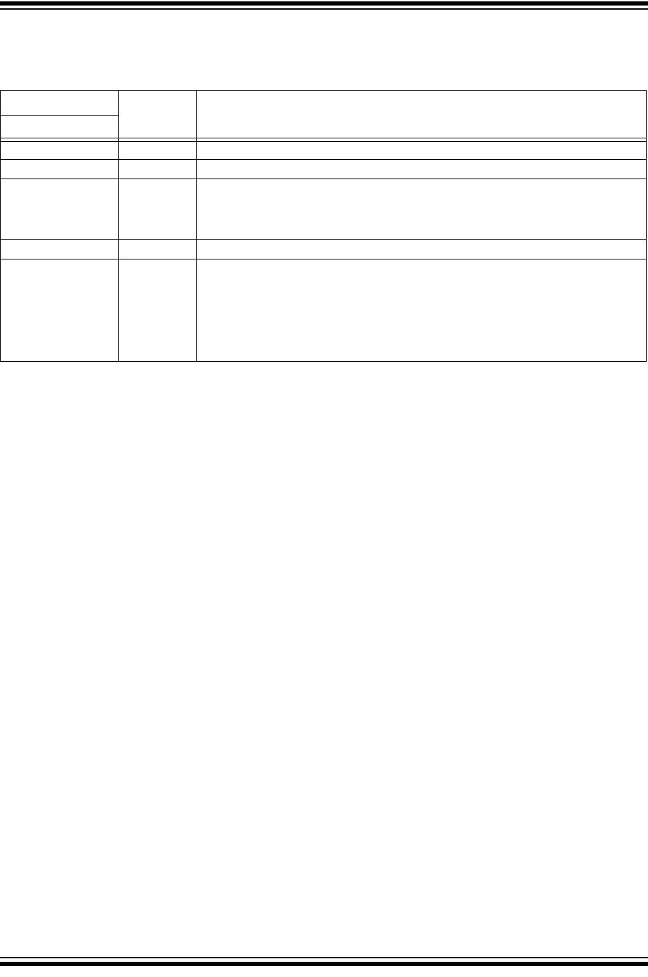
TABLE 3-1: PIN FUNCTION TABLE
3.1 Ground (GND)
The GND pin is the system ground pin. Pin 2 must be
connected to system ground. Pin 1 can also be
connected to system ground which would provide
better thermal conduction to the die.
3.2 Hysteresis Input (HYS)
This is an input pin which can be connected to V
DD
or
GND to select output hysteresis. Either 2°C
(HYST = GND) or 10°C (HYST = V
DD
)
of typical
hysteresis can be selected.
3.3 Power Pin (V
DD
)
The operating voltage range, as specified in the DC
electrical specification table, is applied on this pin.
3.4 Switch Output (Output)
This output is triggered when temperature rises or falls
beyond the programmed trip temperature threshold.
MCP9501/3 require an external pull-up resistor.
MCP9501/2/3/4
Symbol Description
SOT-23-5
1 GND Ground
2 GND Ground (must be connected to ground)
3 HYST Hysteresis Selection Input:
HYST = GND → Hysteresis is 2°C (typical)
HYST = V
DD
→ Hysteresis is 10°C (typical)
4V
DD
Power pin
5 Output Output Options:
MCP9501 → Open-Drain, Active-Low Output (Hot-Option)
MCP9502 → Push-Pull, Active-High Output (Hot-Option)
MCP9503 → Open-Drain, Active-Low Output (Cold-Option)
MCP9504 → Push-Pull, Active-High Output (Cold-Option)