SMF5.0AT1 Series
http://onsemi.com
3
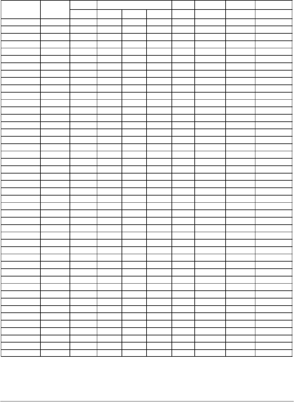
ELECTRICAL CHARACTERISTICS (T
L
= 30°C unless otherwise noted, V
F
= 1.25 Volts @ 200 mA)
V
RWM
(V) V
BR
@ I
T
(V) (Note 6) I
T
I
R
@ V
RWM
V
C(Max)
I
PP(Max)
(A)
Device Marking
(Note 5) Min Nom Max (mA) (A) (V) (Note 7)
SMF5.0A KE 5 6.4 6.7 7 10 400 9.2 21.7
SMF6.0A KG 6 6.67 7.02 7.37 10 400 10.3 19.4
SMF6.5A KK 6.5 7.22 7.6 7.98 10 250 11.2 17.9
SMF7.0A KM 7 7.78 8.2 8.6 10 100 12 16.7
SMF7.5A KP 7.5 8.33 8.77 9.21 1 50 12.9 15.5
SMF8.0A KR 8 8.89 9.36 9.83 1 25 13.6 14.7
SMF8.5A KT 8.5 9.44 9.92 10.4 1 10 14.4 13.9
SMF9.0A KV 9 10 10.55 11.1 1 5 15.4 13.0
SMF10A KX 10 11.1 11.7 12.3 1 2.5 17 11.8
SMF11A KZ 11 12.2 12.85 13.5 1 2.5 18.2 11.0
SMF12A LE 12 13.3 14 14.7 1 2.5 19.9 10.1
SMF13A LG 13 14.4 15.15 15.9 1 1 21.5 9.3
SMF14A LK 14 15.6 16.4 17.2 1 1 23.2 8.6
SMF15A LM 15 16.7 17.6 18.5 1 1 24.4 8.2
SMF16A LP 16 17.8 18.75 19.7 1 1 26 7.7
SMF17A LR 17 18.9 19.9 20.9 1 1 27.6 7.2
SMF18A LT 18 20 21 22.1 1 1 29.2 6.8
SMF20A LV 20 22.2 23.35 24.5 1 1 32.4 6.2
SMF22A LX 22 24.4 25.6 26.9 1 1 35.5 5.6
SMF24A LZ 24 26.7 28.1 29.5 1 1 38.9 5.1
SMF26A ME 26 28.9 30.4 31.9 1 1 42.1 4.8
SMF28A MG 28 31.1 32.8 34.4 1 1 45.4 4.4
SMF30A MK 30 33.3 35.1 36.8 1 1 48.4 4.1
SMF33A MM 33 36.7 38.7 40.6 1 1 53.3 3.8
SMF36A MP 36 40 42.1 44.2 1 1 58.1 3.4
SMF40A MR 40 44.4 46.8 49.1 1 1 64.5 3.1
SMF43A MT 43 47.8 50.3 52.8 1 1 69.4 2.9
SMF45A MV 45 50 52.65 55.3 1 1 72.7 2.8
SMF48A MX 48 53.3 56.1 58.9 1 1 77.4 2.6
SMF51A MZ 51 56.7 59.7 62.7 1 1 82.4 2.4
SMF54A NE 54 60 63.15 66.3 1 1 87.1 2.3
SMF58A NG 58 64.4 67.8 71.2 1 1 93.6 2.1
SMF60A NK 60 66.7 70.2 73.7 1 1 96.8 1.8
SMF64A NM 64 71.1 74.85 78.6 1 1 103 1.7
SMF70A NP 70 77.8 81.9 86 1 1 113 1.5
SMF75A NR 75 83.3 87.7 92.1 1 1 121 1.4
SMF78A NT 78 86.7 91.25 95.8 1 1 126 1.4
SMF85A NV 85 94.4 99.2 104 1 1 137 1.3
SMF90A NX 90 100 105.5 111 1 1 146 1.2
SMF100A NZ 100 111 117 123 1 1 162 1.1
SMF110A PE 110 122 128.5 135 1 1 177 1.0
SMF120A PG 120 133 140 147 1 1 193 0.9
SMF130A PK 130 144 151.5 159 1 1 209 0.8
SMF150A PM 150 167 176 185 1 1 243 0.7
SMF160A PP 160 178 187.5 197 1 1 259 0.7
SMF170A PR 170 189 199 209 1 1 275 0.6
5. A transient suppressor is normally selected according to the Working Peak Reverse Voltage (V
RWM
) which should be equal to or greater
than the DC or continuous peak operating voltage level.
6. V
BR
measured at pulse test current I
T
at ambient temperature of 25°C.
7. Surge current waveform per Figure 2 and derate per Figure 3.