VS-ST650C24L1

VS-ST650C..L Series
www.vishay.com
Vishay Semiconductors
Revision: 15-Apr-14
4
Document Number: 93738
For technical questions within your region: DiodesAmericas@vishay.com
, DiodesAsia@vishay.com, DiodesEurope@vishay.com
THIS DOCUMENT IS SUBJECT TO CHANGE WITHOUT NOTICE. THE PRODUCTS DESCRIBED HEREIN AND THIS DOCUMENT
ARE SUBJECT TO SPECIFIC DISCLAIMERS, SET FORTH AT www.vishay.com/doc?91000
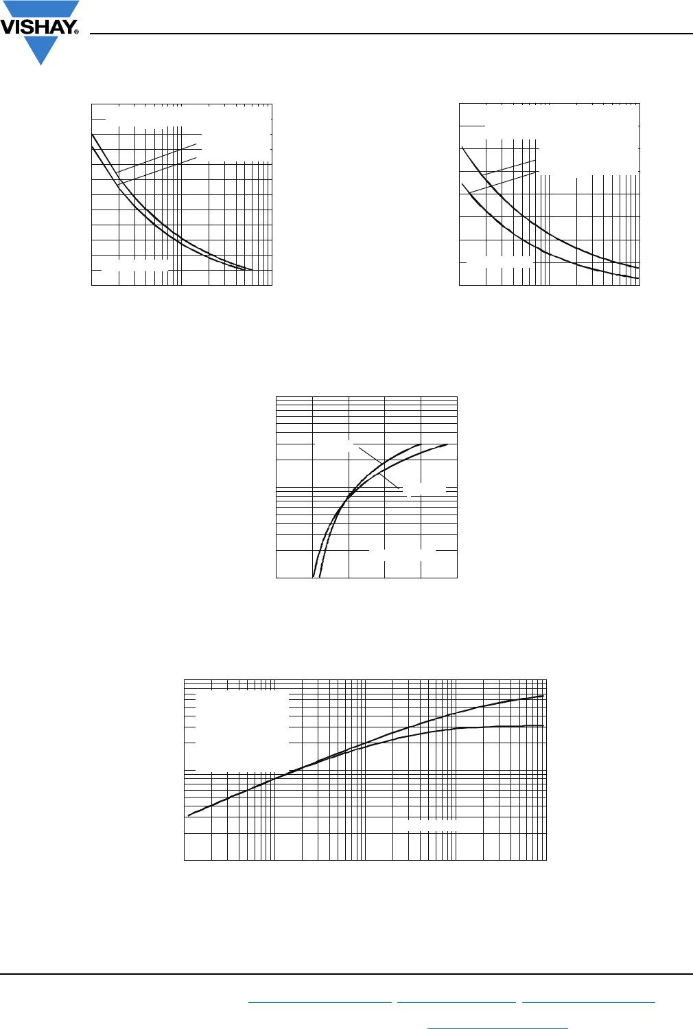
Fig. 1 - Current Ratings Characteristics
Fig. 2 - Current Ratings Characteristics
Fig. 3 - Current Ratings Characteristics
Fig. 4 - Current Ratings Characteristics
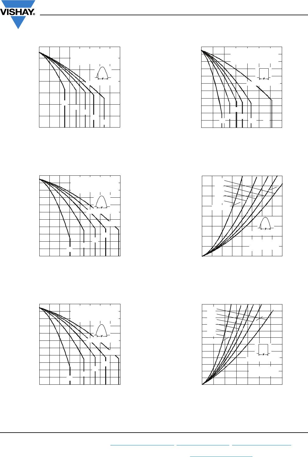
Fig. 5 - On-State Power Loss Characteristics
Fig. 6 - On-State Power Loss Characteristics
60
70
80
90
100
110
120
130
0 50 100 150 200 250 300 350 400
30°
60°
90°
120°
180°
Av era g e O n-state C urren t (A )
Conduction Angle
Maxim um Allowable Heatsink TemperatureC)
ST 650C ..L Se rie s
(Single Side C oo le d)
R (D C) = 0.07 3 K/W
th J-hs
20
30
40
50
60
70
80
90
100
110
120
130
0 100 200 300 400 500 600 700 800
30°
60°
90°
120°
180°
Av era g e On-sta te C urre nt (A)
Conduction Angle
Maximum Allowable Heatsink Temperature (°C)
ST 650C ..L Se ries
(Double Side Cooled)
R (D C ) = 0.0 31 K/W
thJ-h s
20
30
40
50
60
70
80
90
100
110
120
130
0 100 200 300 400 500 600 700 800
30°
60°
90°
120°
180°
Av era g e On-sta te C urre nt (A)
Conduction Angle
Maximum Allowable Heatsink Temperature (°C)
ST 650C ..L Se ries
(Double Side Cooled)
R (D C ) = 0.0 31 K/W
thJ-h s
20
30
40
50
60
70
80
90
100
110
120
130
0 200 400 600 800 1000 1200 1400
DC
30°
60°
90°
120°
180°
Average O n-state Current (A)
Cond uction Period
Maxim um Allow able Heatsink Tem perature (°C)
ST650C..L Series
(D ouble Side C ooled)
R (DC ) = 0.031 K/W
th J-hs
0
250
500
750
1000
1250
1500
1750
2000
0 100 200 300 400 500 600 700 800
RMS Lim it
Conduction Angle
180°
120°
90°
60°
30°
Maximum Average On-state Power Loss (W)
Average On-state Current (A)
ST650C..L Series
T = 125°C
J
0
200
400
600
800
1000
1200
1400
1600
1800
2000
2200
2400
0 200 400 600 800 1000 1200 1400
DC
180°
120°
90°
60°
30°
RMS Lim it
Conduction Period
M axim um Average On-state Pow er Loss (W)
A ve rag e O n -sta te C urre nt (A)
ST650C ..L Series
T = 125°C
J
VS-ST650C..L Series
www.vishay.com
Vishay Semiconductors
Revision: 15-Apr-14
5
Document Number: 93738
For technical questions within your region: DiodesAmericas@vishay.com
, DiodesAsia@vishay.com, DiodesEurope@vishay.com
THIS DOCUMENT IS SUBJECT TO CHANGE WITHOUT NOTICE. THE PRODUCTS DESCRIBED HEREIN AND THIS DOCUMENT
ARE SUBJECT TO SPECIFIC DISCLAIMERS, SET FORTH AT www.vishay.com/doc?91000
Fig. 7 - Maximum Non-Repetitive Surge Current
Single and Double Side Cooled
Fig. 8 - Maximum Non-Repetitive Surge Current
Single and Double Side Cooled
Fig. 9 - On-State Voltage Drop Characteristics
Fig. 10 - Thermal Impedance Z
thJ-hs
Characteristics
4000
5000
6000
7000
8000
9000
10000
001011
Number O f Equal Amp litude Half Cycle Current Pulses (N)
Pea k Half Sine W ave On-state Current (A)
A t Any R ated Loa d C ond itio n An d W ith
R a t e d V A p p lie d F ollo w in g Su rg e .
RRM
Initial T = 12 5°C
@ 60 Hz 0 .0083 s
@ 50 Hz 0 .0100 s
J
ST650 C..L S erie s
4000
5000
6000
7000
8000
9000
10000
11000
12000
11.010.0
Peak Half Sine W ave O n-state C urre nt (A)
Pulse Train Duration (s)
M a xim um N o n Re p etitive Surg e C urre nt
Ve rsus Pulse Tra in D ura tion . C o ntrol
O f C onductio n M ay Not Be M aintained.
In it ia l T = 1 2 5 ° C
N o V o lt a g e R e a p p lie d
Ra te d V Re a p p lied
RRM
J
ST650C..L Series
100
1000
10000
0.5 1 1.5 2 2.5 3
Instantaneous On-state Current (A)
Instan tan eous O n -stat e Voltage (V)
ST650C..L Series
T = 25°C
J
T = 125°C
J
0.001
0.01
0.1
0111.010.0100.0
Square Wave Pulse Duration (s)
thJ-hs
Stea d y Sta te Va lu e
R = 0.073 K/W
(Sin gle Sid e C oo le d)
R = 0.031 K/W
(Do uble Side Cooled)
(DC Operatio n)
thJ-hs
thJ-hs
Transient Th erm al Im pe d ance Z (K/W )
ST650C ..L Se ries
VS-ST650C..L Series
www.vishay.com
Vishay Semiconductors
Revision: 15-Apr-14
6
Document Number: 93738
For technical questions within your region: DiodesAmericas@vishay.com
, DiodesAsia@vishay.com, DiodesEurope@vishay.com
THIS DOCUMENT IS SUBJECT TO CHANGE WITHOUT NOTICE. THE PRODUCTS DESCRIBED HEREIN AND THIS DOCUMENT
ARE SUBJECT TO SPECIFIC DISCLAIMERS, SET FORTH AT www.vishay.com/doc?91000
Fig. 11 - Gate Characteristics
ORDERING INFORMATION TABLE
0.1
1
10
100
0.001 0.01 0.1 1 10 100
VG D
IG D
(b)
(a)
Tj = 2 5 ° C
Tj=125 °C
Tj=-40 °C
(2) (3)
Instantan eo us G a te C urren t (A)
Insta nt an e ous G a te V olta g e (V )
a) Recom mended load line for
b ) R e c o m m e n d e d lo a d li n e f o r
<=30% rated di/dt : 10V, 10ohm s
Frequency Limited by PG(AV)
rated di/dt : 20V, 10ohm s; tr<=1 µs
tr<=1 µs
(1)
(1) PG M = 10W , tp = 4m s
(2) PG M = 20W , tp = 2m s
(3) PG M = 40W , tp = 1m s
(4) PG M = 60W , tp = 0.66m s
Rectangular gate pulse
ST6 50C..L Se rie s
(4)
- Thyristor
2
- Essential part number
3
- 0 = Converter grade
4
- C = Ceramic PUK
9 - Critical dV/dt:
5
- Voltage code x 100 = V
RRM
(see Voltage Ratings table)
6
- L = PUK case TO-200AC (B-PUK)
7
8
- 0 = Eyelet terminals (gate and auxiliary cathode unsoldered leads)
1 = Fast-on terminals (gate and auxiliary cathode unsoldered leads)
2 = Eyelet terminals (gate and auxiliary cathode soldered leads)
3 = Fast-on terminals (gate and auxiliary cathode soldered leads)
None = 500 V/µs (standard selection)
L = 1000 V/µs (special selection)
Device code
51 32 4 6 7 8 9
STVS- 65 0 C 24 L 1 -
1
- Vishay Semiconductors product
LINKS TO RELATED DOCUMENTS
Dimensions www.vishay.com/doc?95076

VS-ST650C24L1

Mfr. #:
Manufacturer:
Vishay Semiconductors
Description:
SCR Modules 2400 Volt 790 Amp
Lifecycle:
New from this manufacturer.
Delivery:
DHL FedEx Ups TNT EMS
Payment:
T/T Paypal Visa MoneyGram Western Union