DG9408E, DG9409E
www.vishay.com
Vishay Siliconix
S16-1452-Rev. A, 25-Jul-16
1
Document Number: 75375
For technical questions, contact: analogswitchtechsupport@vishay.com
THIS DOCUMENT IS SUBJECT TO CHANGE WITHOUT NOTICE. THE PRODUCTS DESCRIBED HEREIN AND THIS DOCUMENT
ARE SUBJECT TO SPECIFIC DISCLAIMERS, SET FORTH AT www.vishay.com/doc?91000
3.2 , Fast Switching Speed, +12 V / +5 V / +3 V / ± 5 V,
4- / 8-Channel Analog Multiplexers
DESCRIPTION
The DG9408E, DG9409E uses BiCMOS wafer fabrication
technology that allows the DG9408E, DG9409E to operate
on single and dual supplies. Single supply voltage
ranges from 3 V to 16 V while dual supply operation is
recommended with ± 3 V to ± 8 V.
The DG9408E is an 8-channel single-ended analog
multiplexer designed to connect one of eight inputs to a
common output as determined by a 3-bit binary address
(A
0
, A
1
, A
2
). The DG9409E is a dual 4-channel differential
analog multiplexer designed to connect one of four
differential inputs to a common dual output as determined
by its 2-bit binary address (A
0
, A
1
). Break-before-make
switching action to protect against momentary crosstalk
between adjacent channels.
As a committed partner to the community and the
environment, Vishay Siliconix manufactures this product
with lead (Pb)-free device terminations. The DG9408E,
DG9409E are offered in a QFN package that has a
nickel-palladium-gold device terminations and is
represented by the lead (Pb)-free “-E4” suffix. The
nickel-palladium-gold device terminations meet all the
JEDEC
®
standards for reflow and MSL ratings.
FEATURES
• 3 V to 16 V single supply or ± 3 V to ± 8 V dual
supply operation
• Low on-resistance - R
ON
: 3.2 typ.
• Fast switching: t
ON
- 36 ns, t
OFF
- 24 ns
• Break-before-make guaranteed
• Low leakage
• TTL, CMOS, LV logic (3 V) compatible
• 2500 V ESD protection (HBM)
• Material categorization: for definitions of compliance
please see www.vishay.com/doc?99912
BENEFITS
• Fast switching speed
• Low switch resistance
• Wide operation voltage range
• Simple logic interface
APPLICATIONS
• Automatic test equipment
• Process control and automation
• Data acquisition systems
• Meters and instruments
• Medical and healthcare systems
• Communication systems
• Audio and video signal routing
• Relay replacement
• Battery powered systems
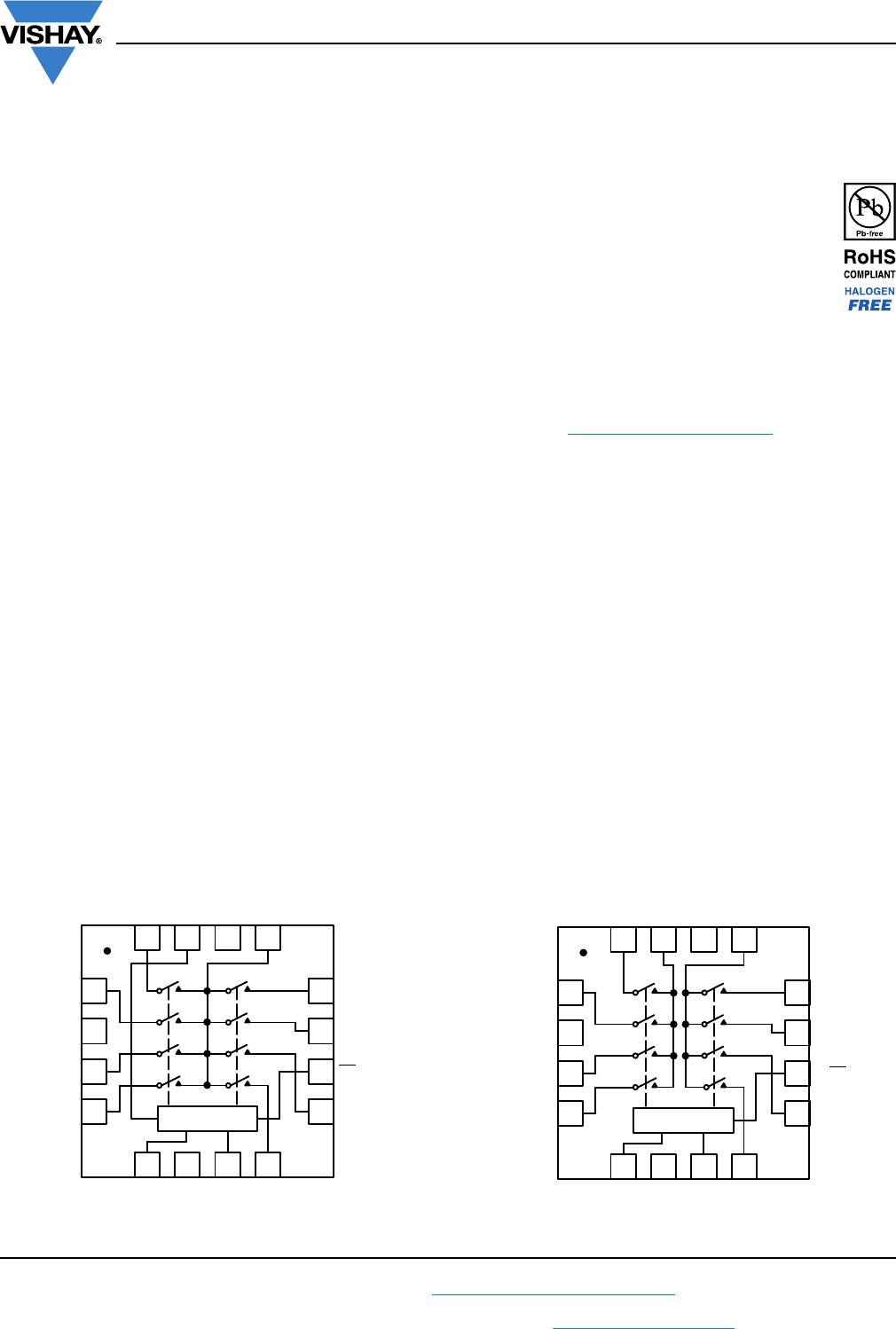
FUNCTIONAL BLOCK DIAGRAM AND PIN CONFIGURATION
Note
• QFN16 package central exposed pad has no electrical connection inside the chip. It can be connected GND, V+, V-, or left floating.
49
GND S
2a
S
4b
S
3b
S
3a
EN
S
2b
S
1a
1
2
3
12
11
10
567
8
16 15 14 13
A
0
V+ A
1
S
4a
S
1b
D
b
V- D
a
Decoder / driver
Top view
DG9409E
QFN16
5
GND S
6
S
4
S
3
S
7
EN
S
2
S
5
1
2
3
12
11
10
49
5678
16 15 14 13
A
0
V+ A
1
S
8
S
1
A
2
V- D
Decoder / driver
Top view
DG9408E
QFN16