General Description
The MAX4122–MAX4129 family of operational amplifiers
combines wide bandwidth and excellent DC accuracy with
Rail-to-Rail
®
operation at the inputs and outputs. These
devices require only 650µA per amplifier, and operate from
either a single supply (+2.7V to +6.5V) or dual supplies
(±1.35V to ±3.25V) with a common-mode voltage range
that extends 250mV beyond V
EE
and V
CC
. They are capa-
ble of driving 250 loads. The MAX4122/MAX4123/
MAX4126/MAX4127/MAX4129 have a 5MHz gain band-
width product, while the decompensated MAX4124/
MAX4125/MAX4128 (stable at closed-looped gains of
10 or greater) have a 25MHz gain bandwidth product. In
addition, the MAX4123/MAX4125/MAX4127 feature a
shutdown mode in which the outputs are placed in a
high-impedance state and the supply current is reduced
to only 25µA per amplifier.
With their rail-to-rail input common-mode range and
output swing, these amplifiers are ideal for low-voltage
single-supply operation. Although the minimum operat-
ing voltage is specified at 2.7V, the devices typically
operate down to 1.8V. In addition, low offset voltage
and high speed make them the ideal signal-condition-
ing stages for precision, low-voltage, data-acquisition
systems. The MAX4122 and MAX4124 come in the
space-saving 5-pin SOT23-5 package.
________________________Applications
Battery-Powered Instruments
Portable Equipment
Data-Acquisition Systems
Signal Conditioning
Low-Power, Low-Voltage Applications
Features
5-Pin SOT23 Package (MAX4122/4)
+2.7V to +6.5V Single-Supply Operation
Rail-to-Rail Input Common-Mode Voltage Range
Rail-to-Rail Output Voltage Swing
5MHz Gain-Bandwidth Product (MAX4122/3/6/7/9)
25MHz Gain-Bandwidth Product (MAX4124/5/8)
650µA Quiescent Current per Amplifier
25µA Shutdown Function (MAX4123/5/7)
200µV Offset Voltage
No Phase Reversal for Overdriven Inputs
Drive 250Loads
Stable with 500pF Capacitive Loads
Unity-Gain Stable (MAX4122/3/6/7/9)
Stable at Gains 10V/V (MAX4124/5/8)
MAX4122–MAX4129
Single/Dual/Quad, Wide-Bandwidth, Low-Power,
Single-Supply Rail-to-Rail I/O Op Amps
________________________________________________________________
Maxim Integrated Products
1
MAX187
MAX4123
SHDN
3
1
2
4
5
6
8
7
V
DD
+5V
AIN
VREF
GND
DOUT
SERIAL
INTERFACE
SCLK
CS
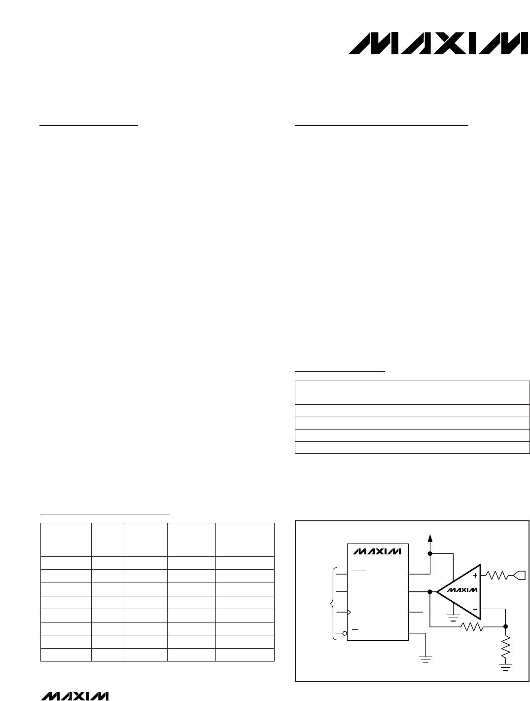
__________Typical Operating Circuit
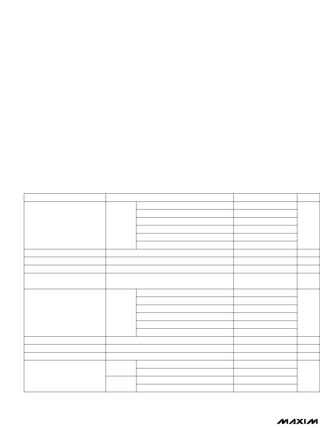
Selection Table
19-1087; Rev 1; 8/97
PART
MAX4122EUK
MAX4123C/D
MAX4123ESA -40°C to +85°C
0°C to +70°C
-40°C to +85°C
TEMP. RANGE
PIN-
PACKAGE
5 SOT23-5
Dice*
8 SO
Ordering Information
Ordering Information continued at end of data sheet.
*
Dice are specified at T
A
= +25°C, DC parameters only.
Pin Configurations appear at end of data sheet.
MARKING
INFO.
AAAZ
BW
(MHz)
AMPS
PER
PKG.
MAX4122 5 1
MAX4123 5 1
PART
MAX4124 25 1
MAX4125 25 1
MAX4126 5 2
MAX4127 5 2
MAX4128 25 2
MAX4129 5 4
SHUT-
DOWN
MODE
Yes
Yes
Yes
PIN-
PACKAGE
5 SOT23-5
8 SO/µMAX
5 SOT23-5
8 SO/µMAX
8 SO/µMAX
14 SO
8 SO/µMAX
14 SO
MAX4123EUA -40°C to +85°C 8 µMAX
For free samples & the latest literature: http://www.maxim-ic.com, or phone 1-800-998-8800.
For small orders, phone 408-737-7600 ext. 3468.
Rail-to-Rail is a registered trademark of Nippon Motorola, Ltd.
MAX4122–MAX4129
Single/Dual/Quad, Wide-Bandwidth, Low-Power,
Single-Supply Rail-to-Rail I/O Op Amps
2 _______________________________________________________________________________________
ABSOLUTE MAXIMUM RATINGS
DC ELECTRICAL CHARACTERISTICS
(V
CC
= +2.7V to +6.5V, V
EE
= 0V, V
CM
= 0V, V
OUT
= V
CC
/2, R
L
tied to V
CC
/2, SHDN 2V (or open), T
A
= +25°C, unless
otherwise noted.)
Stresses beyond those listed under “Absolute Maximum Ratings” may cause permanent damage to the device. These are stress ratings only, and functional
operation of the device at these or any other conditions beyond those indicated in the operational sections of the specifications is not implied. Exposure to
absolute maximum rating conditions for extended periods may affect device reliability.
Supply Voltage (V
CC
-V
EE
).....................................................7.5V
IN+, IN-, SHDN Voltage...................(V
CC
+ 0.3V) to (V
EE
- 0.3V)
Output Short-Circuit Duration (Note 1).......................Continuous
(short to either supply)
Continuous Power Dissipation (T
A
= +70°C)
5-pin SOT23-5 (derate 7.1mW/°C above +70°C) .........571mW
8-pin SO (derate 5.88mW/°C above +70°C).................471mW
8-pin µMAX (derate 4.10mW/°C above +70°C)............330mW
14-pin SO (derate 8.00mW/°C above +70°C)...............640mW
Operating Temperature Range
MAX412_E__ ....................................................-40°C to +85°C
Maximum Junction Temperature .....................................+150°C
Storage Temperature Range.............................-65°C to +160°C
Lead Temperature (soldering, 10sec).............................+300°C
V
CM
= V
EE
to V
CC
MAX4123ESA/MAX4125ESA
CONDITIONS
nA±1 ±12Input Offset Current
nA±50 ±150Input Bias Current
72 80
0.1Output Resistance
k500Differential Input Resistance
78 98
dB78 100Power-Supply Rejection Ratio
UNITSMIN TYP MAXPARAMETER
V
OUT
= 0.4V to 4.6V, R
L
= 250 75 84
dBLarge-Signal Voltage Gain
V
V
EE
- V
CC
+
0.25 0.25
Common-Mode Input
Voltage Range
Note 1: Provided that the maximum package power-dissipation rating is met.
MAX4122EUK/MAX4124EUK ±0.35 ±1.50
MAX4123EUA/MAX4125EUA ±0.35 ±1.20
±0.20 ±0.60
MAX4126ESA/MAX4127ESD/MAX4128ESA
MAX4126EUA/MAX4128EUA ±0.40 ±1.50
MAX4129ESD ±0.35 ±1.50
Input Offset Voltage
±0.25 ±0.75
V
CM
=
V
EE
to V
CC
MAX4123ESA/MAX4125ESA
mV
V
CM
= V
EE
to V
CC
-1.5V < V
DIFF
< 1.5V
V
CC
= 2.7V to 6.5V
A
V
= 1
SHDN < 0.8V, V
OUT
= 0V to V
CC
µA±0.1 ±1Off-Leakage Current
MAX4122EUK/MAX4124EUK
(V
EE
-
0.25) <
V
CM
<
(V
CC
+
0.25V)
67 90
Common-Mode Rejection Ratio
MAX4129ESD
MAX4126EUA/MAX4128EUA
64 84
dB
66 86
MAX4126ESA/MAX4127ESD/MAX4128ESA
MAX4123EUA/MAX4125EUA
74 94
68 88
V
CC
= 5V
V
OUT
= 0.4V to 2.3V, R
L
= 250
V
OUT
= 0.25V to 2.45V, R
L
= 100k
V
OUT
= 0.25V to 4.75V, R
L
= 100k
V
CC
= 2.7V
92 104
94 106
MAX4122–MAX4129
Single/Dual/Quad, Wide-Bandwidth, Low-Power,
Single-Supply Rail-to-Rail I/O Op Amps
_______________________________________________________________________________________ 3
DC ELECTRICAL CHARACTERISTICS
(V
CC
= +2.7V to +6.5V, V
EE
= 0V, V
CM
= 0V, V
OUT
= V
CC
/2, R
L
tied to V
CC
/2, SHDN 2V (or open), T
A
= -40°C to +85°C, unless
otherwise noted.)
DC ELECTRICAL CHARACTERISTICS (continued)
(V
CC
= +2.7V to +6.5V, V
EE
= 0V, V
CM
= 0V, V
OUT
= V
CC
/2, R
L
tied to V
CC
/2, SHDN 2V (or open), T
A
= +25°C, unless
otherwise noted.)
R
L
= 100k
CONDITIONS
20 35
Low
V2.7 6.5Operating Supply-Voltage Range
SHDN > 0.8V,
MAX4123/MAX4125/MAX4127
240 290
12 20
V
OL
- V
EE
125 170
MAX4122/
MAX4123/
MAX4124/
MAX4125
V
0.8
mA50Output Short-Circuit Current
µA
40 60
Shutdown Supply Current
per Amplifier
UNITS
MIN TYP MAX
PARAMETER
V
CC
- V
OH
V
OL
- V
EE
V
CC
- V
OH
R
L
= 250
V
CC
- V
OH
V
OL
- V
EE
V
CC
- V
OH
R
L
= 250
R
L
= 100k
25 40
mV
280 330
15 30
V
OL
- V
EE
Output Voltage Swing
180 230
MAX4126/
MAX4127/
MAX4128/
MAX4129
High 2.0
SHDN Logic Threshold
MAX4123/MAX4125/MAX4127
V
CC
= 5V
MAX4123/MAX4125/MAX4127 µA±1 ±3
SHDN Input Current
V
CC
= 2.7V
V
CM
= V
OUT
= V
CC
/2 µA
650 750
V
CC
= 5V 725 825
Supply Current per Amplifier
V
CC
= 2.7V 25 40
MAX4122EUK/MAX4124EUK
(V
EE
-
0.2V) <
V
CM
<
(V
CC
+
0.2V)
MAX4123ESA/MAX4125ESA
MAX4129ESD
MAX4122EUK/MAX4124EUK
MAX4123ESA/MAX4125ESA
CONDITIONS
±3.50
62
V
CM
= V
EE
to V
CC
MAX4123EUA/MAX4125EUA
V
V
EE
- V
CC
+
0.20 0.20
Common-Mode Input
Voltage Range
mV
±4.40
±0.75
MAX4126ESA/MAX4127ESD/MAX4128ESA
MAX4126EUA/MAX4128EUA ±4.70
MAX4129ESD
Common-Mode Rejection Ratio
±4.00
Input Offset Voltage
±0.95
V
CM
=
V
EE
to V
CC
nA±18
MAX4126EUA/MAX4128EUA
Input Offset Current
µV/°C±2
60
dB
58
MAX4126ESA/MAX4127ESD/MAX4128ESA
Input Offset Voltage Tempco
MAX4123EUA/MAX4125EUA
74
60
76
UNITSMIN TYP MAXPARAMETER
V
CM
= V
EE
to V
CC
nA±160Input Bias Current

MAX4122EUK+T

Mfr. #:
Manufacturer:
Maxim Integrated
Description:
Operational Amplifiers - Op Amps Single Wide-Bandwdth Single-Supply R-R
Lifecycle:
New from this manufacturer.
Delivery:
DHL FedEx Ups TNT EMS
Payment:
T/T Paypal Visa MoneyGram Western Union