PS8802-1,-2
*1 Test circuit for propagation delay time
Input
Output
50%
1.5 V
V
OL
tPHL tPLH
(IF = 7.5 mA)
Pulse input (I
F)
(PW = 1 s,
Duty cycle = 1/10)
V
O (Monitor)
V
CC = 5 V
Input
(Monitor)
0.1 F
CL = 15 pF
47 Ω
R
L = 2.2 kΩ
PS8802-1
μ
μ
Pulse input (IF)
(PW = 1 s,
Duty cycle = 1/10)
V
O (Monitor)
V
CC = 5 V
Input
(Monitor)
0.1 F
CL = 15 pF
47 Ω
R
L = 2.2 kΩ
PS8802-2
μ
μ
Remark C
L is approximately 15 pF which includes probe and stray wiring capacitance.
*2 Test circuit for common mode transient immunity
I
F
V
O
(Monitor)
V
CC
= 5 V
0.1 F
R
L
= 4.1 kΩ
PS8802-1
V
CM
μ
C
L
= 15 pF
I
F
V
O
(Monitor)
V
CC
= 5 V
0.1 F
R
L
= 4.1 kΩ
PS8802-2
V
CM
SW
μ
C
L
= 15 pF
90%
10%
1.5 kV
0 V
V
OH
2 V
0.8 V
V
OL
V
CM
V
O
(I
F
= 0 mA)
V
O
(I
F
= 16 mA)
t
r
t
f
USAGE CAUTIONS
1. This product is weak for static electricity by designed with high-speed integrated circuit so protect against static
electricity when handling.
2. By-pass capacitor of 0.1
μ
F is used between VCC and GND near device. Also, ensure that the distance between
the leads of the photocoupler and capacitor is no more than 10 mm.
3. Avoid storage at a high temperature and high humidity.
Data Sheet PN10418EJ07V0DS
7
PS8802-1,-2
TYPICAL CHARACTERISTICS (TA = 25°C, unless otherwise specified)
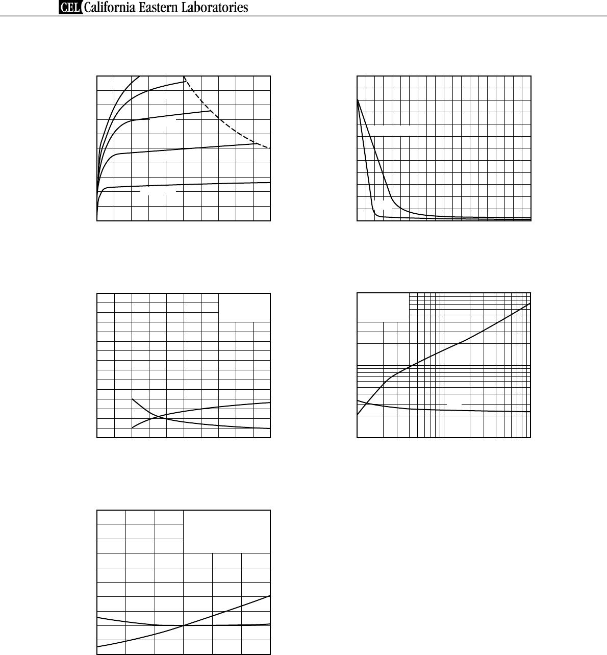
50
30
20
10
0
40
25 50 75 100
Ambient Temperature T
A (˚C)
Diode Power Dissipation PD (mW)
DIODE POWER DISSIPATION vs.
AMBIENT TEMPERATURE
120
100
60
20
0
80
40
25 50 75 100
Ambient Temperature T
A (˚C)
Transistor Power Dissipation PC (mW)
TRANSISTOR POWER DISSIPATION vs.
AMBIENT TEMPERATURE
100
0.01
0.1
10
1
1.4 1.8 2.0 2.41.0 1.2 1.6 2.2
Forward Voltage V
F (V)
Forward Current IF (mA)
FORWARD CURRENT vs.
FORWARD VOLTAGE
TA = +100˚C
+50˚C
+25˚C
0˚C
–25˚C
80
20
0
40
60
70
50
10
30
0.5 5 10 501
V
CC = 4.5 V,
V
O = 0.4 V
Forward Current IF (mA)
CURRENT TRANSFER RATIO vs.
FORWARD CURRENT
Current Transfer Ratio CTR (
%
)
1.6
0.0
1.2
0.4
1.4
1.0
0.8
0.6
0.2
0 50 100–50 –25 25
75
Ambient Temperature T
A (˚C)
Normalized Current Transfer Raio CTR
NORMALIZED CURRENT TRANSFER
RATIO vs. AMBIENT TEMPERATURE
Normalized to 1.0
at T
A = 25˚C, IF = 16 mA,
V
CC = 4.5 V, VO = 0.4 V
Ambient Temperature T
A (˚C)
High Level Output Current IOH (nA)
HIGH LEVEL OUTPUT CURRENT vs.
AMBIENT TEMPERATURE
10 000
10
0.1
1 000
100
50 100–25 0 25 75
VCC = VO = 30 V
V
CC = VO = 5.5 V
1
I
F = 0 mA
Remark The graphs indicate nominal characteristics.
Data Sheet PN10418EJ07V0DS
8
PS8802-1,-2
10
4
0
8
6
2
4 8 18 20162 6 10 12 14
20 mA
15 mA
10 mA
I
F
= 5 mA
25 mA
Output Voltage V
O
(V)
Output Current I
O
(mA)
OUTPUT CURRENT vs.
OUTPUT VOLTAGE
5
4
2
0
3
1
–50 0 50
100
–25
7525
Ambient Temperature T
A
(˚C)
NORMALIZED PROPAGATION DELAY TIME
vs. AMBIENT TEMPERATURE
Normalized Propagation Delay Time t
PHL
, t
PLH
Normalized to 1.0
at T
A
= 25˚C,
I
F
= 16 mA, V
CC
= 5 V,
R
L
= 2.2 kΩ
t
PLH
t
PHL
Forward Current I
F
(mA)
PROPAGATION DELAY TIME vs.
FORWARD CURRENT
Propagation Delay Time t
PHL
, t
PLH
( s)
μ
3.0
0
1.0
2.0
10 15
25
5
20
t
PHL
t
PLH
V
CC
= 5 V,
R
L
= 2.2 kΩ,
CTR : 25
%
Load Resistance R
L
(Ω)
PROPAGATION DELAY TIME vs.
LOAD RESISTANCE
Propagation Delay Time t
PHL
, t
PLH
( s)
μ
V
CC
= 5 V,
I
F
= 16 mA,
CTR : 25
%
t
PLH
t
PHL
10
1
0.1
10 k
100 k
1 k
Forward Current I
F
(mA)
Output Voltage V
O
(V)
OUTPUT VOLTAGE vs.
FORWARD CURRENT
6
5
4
2
0
3
1
12
16
20
4826
10
14
18
R
L
= 2.2 kΩ
5.6 kΩ
Remark The graphs indicate nominal characteristics.
Data Sheet PN10418EJ07V0DS
9

PS8802-2-F3-AX

Mfr. #:
Manufacturer:
CEL
Description:
High Speed Optocouplers SGL Tr DC Fast Couplr
Lifecycle:
New from this manufacturer.
Delivery:
DHL FedEx Ups TNT EMS
Payment:
T/T Paypal Visa MoneyGram Western Union