MUSES72320
– 2 –
Ver. 0.6E
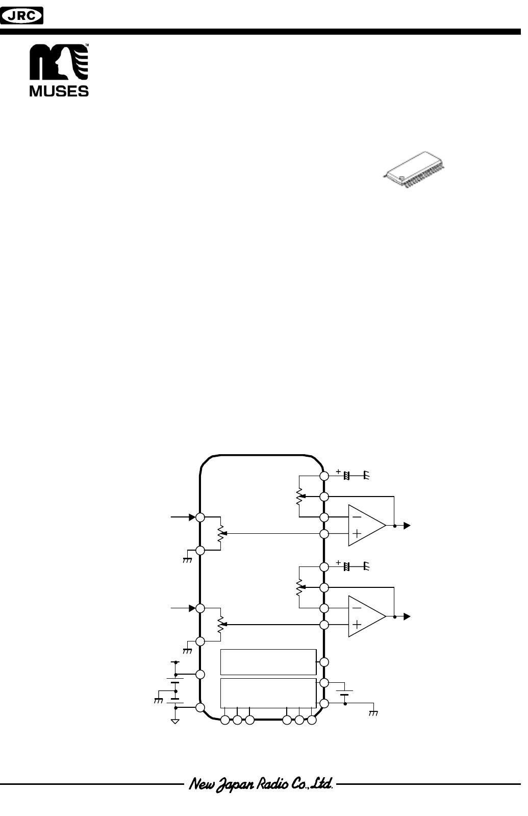
■ PIN FUNCTION
No. SYMBOL FUNCTION No. SYMBOL FUNCTION
1 Z/C REFL
Lch Zero Cross Detection circuit
Reference Voltage
17 D_VDD Digital block Power Supply
2 L_REF Lch Reference Voltage 18 DATA Control data signal input
3 L+
Lch Opamp non-inverting input
connect terminal
19 CLOCK Clock signal input
4 L_REF Lch Reference Voltage 20 LATCH Latch signal input
5 L-
Lch Opamp inverting input connect
terminal
21 D_REF Digital block Reference Voltage
6 L_REF Lch Reference Voltage 22 V+ Power Supply (+)
7 OutL Lch output 23 InR Rch input
8 DCCAP_L
Switching noise rejection capacitor
Lch)
24 V+ Power Supply (+)
9 DCCAP_R
Switching noise rejection capacitor
Rch)
25 V - Power Supply (-)
10 OutR Rch output 26 InL Lch input
11 R_REF Rch Reference Voltage 27 V - Power Supply (-)
12 R-
Rch Opamp inverting input connect
terminal
28 D_CAP
Digital block Noise Rejection
Capacitor terminal
13 R_REF Rch Reference Voltage 29 ADR2 Chip address setting terminal 2
14 R+
Rch Opamp non-inverting input
connect terminal
30 ADR1 Chip address setting terminal 1
15 R_REF Rch Reference Voltage 31 ADR0 Chip address setting terminal 0
16 Z/C REFR
Rch Zero Cross Detection circuit
Reference Voltage
32 Z/C
Zero Cross Detection circuit ON/OFF
setting terminal
116
1732