REV. 0
–12–
AD7708/AD7718
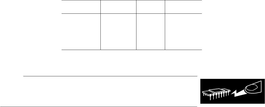
PIN FUNCTION DESCRIPTIONS
Pin No Mnemonic Function
1 AIN7 Analog Input Channel 7. Programmable-gain analog input that can be used as a pseudo-
differential input when used with AINCOM, or as the positive input of a fully-differential input
pair when used with AIN8. (See ADC Control Register section.)
2 AIN8 Analog Input Channel 8. Programmable-gain analog input that can be used as a pseudo-
differential input when used with AINCOM, or as the negative input of a fully-differential input
pair when used with AIN7. (See ADC Control Register section.)
3AV
DD
Analog Supply Voltage
4 AGND Analog Ground
5 REFIN1(–) Negative Reference Input. This reference input can lie anywhere between AGND and AV
DD
– 1 V.
6 REFIN1(+) Positive reference input. REFIN(+) can lie anywhere between AV
DD
and AGND. The nominal
reference voltage [REFIN(+)–REFIN(–)] is 2.5 V but the part is functional with a reference
range from 1 V to AV
DD
.
7 AIN1 Analog Input Channel 1. Programmable-gain analog input that can be used as a pseudo-
differential input when used with AINCOM, or as the positive input of a fully-differential input
pair when used with AIN2. (See ADC Control Register Section.)
8 AIN2 Analog Input Channel 2. Programmable-gain analog input that can be used as a pseudo-
differential input when used with AINCOM, or as the negative input of a fully-differential input
pair when used with AIN1. (See ADC Control Register section.)
9 AIN3 Analog Input Channel 3. Programmable-gain analog input that can be used as a pseudo-
differential input when used with AINCOM, or as the positive input of a fully-differential input
pair when used with AIN4. (See ADC Control Register section.)
10 AIN4 Analog Input Channel 4. Programmable-gain analog input that can be used as a pseudo-
differential input when used with AINCOM, or as the negative input of a fully-differential input
pair when used with AIN3. (See ADC Control Register section.)
11 AIN5 Analog Input Channel 5. Programmable-gain analog input that can be used as a pseudo-
differential input when used with AINCOM, or as the positive input of a fully-differential input
pair when used with AIN6. (See ADC Control Register section ADCCON.)
12 AINCOM All analog inputs are referenced to this input when configured in pseudo-differential input mode.
13 REFIN2(+)/AIN9 Positive reference input/analog input. This input can be configured as a reference input with the
same characteristics as REFIN1(+) or as an additional analog input. When configured as an
analog input this pin provides a programmable-gain analog input that can be used as a pseudo-
differential input when used with AINCOM, or as the positive input of a fully-differential input
pair when used with AIN10. (See ADC Control Register section.)
14 REFIN2(–)/AIN10 Negative reference input/analog input. This pin can be configured as a reference or analog input.
When configured as a reference input it provides the negative reference input for REFIN2.
When configured as an analog input it provides a programmable-gain analog input that can be
used as a pseudo-differential input when used with AINCOM, or as the negative input of a fully-
differential input pair when used with AIN9. (See ADC Control Register section.)
15 AIN6 Analog Input Channel 6. Programmable-gain analog input that can be used as a pseudo-
differential input when used with AINCOM, or as the negative input of a fully-differential input
pair when used with AIN5. (See ADC Control Register section.)
16 P2 P2 can act as a general-purpose Input/Output bit referenced between AV
DD
and AGND. There
is a weak pull-up to AV
DD
internally on this pin.
17 AGND It is recommended that this pin be tied directly to AGND.
18 P1 P1 can act as a general-purpose Input/Output bit referenced between AV
DD
and AGND. There
is a weak pull-up to AV
DD
internally on this pin.
19 RESET Digital input used to reset the ADC to its power-on-reset status. This pin has a weak pull-up
internally to DV
DD
.
20 SCLK Serial clock input for data transfers to and from the ADC. The SCLK has a Schmitt-trigger
input making an opto-isolated interface more robust. The serial clock can be continuous with all
data transmitted in a continuous train of pulses. Alternatively, it can be a noncontinuous clock
with the information being transmitted to or from the AD7708/AD7718 in smaller batches of data.