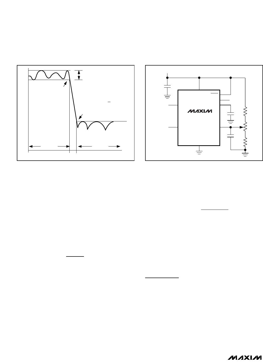
MAX7400/MAX7403/MAX7404/MAX7407
8th-Order, Lowpass, Elliptic,
Switched-Capacitor Filters
______________________________________________________________________________________ 11
with V
COM
= V
DD
/ 2 (typical), and where (V
IN
- V
COM
)
is lowpass filtered by the SCF, and V
OS
is added at the
output stage. See the
Electrical Characteristics
for
COM and OS input voltage ranges. Changing the volt-
age on COM or OS significantly from midsupply
reduces the filter’s dynamic range.
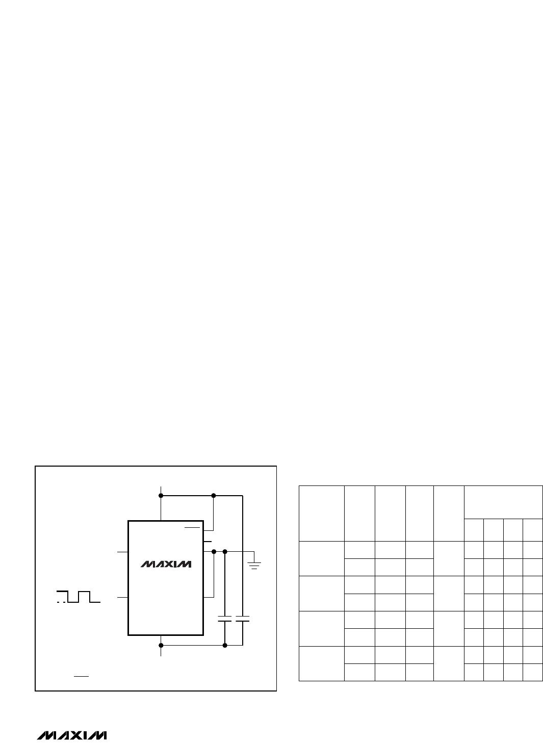
Power Supplies
The MAX7400/MAX7403 operate from a single +5V
supply. The MAX7404/MAX7407 operate from a single
+3V supply. Bypass V
DD
to GND with a 0.1µF capaci-
tor. If dual supplies are required, connect COM to the
system ground and GND to the negative supply. Figure
5 shows an example of dual-supply operation. Single-
supply and dual-supply performance are equivalent.
For single-supply or dual-supply operation, drive CLK
and SHDN from GND (V- in dual-supply operation) to
V
DD
. For a ±2.5V supply, use the MAX7400 or MAX7403;
for a ±1.5V supply, use MAX7404 or MAX7407. For ±5V
dual-supply applications, use the MAX291–MAX297.
Input Signal Amplitude Range
The ideal input signal range is determined by observ-
ing the voltage level at which the total harmonic
distortion plus noise (THD+N) is minimized for a given
corner frequency. The
Typical Operating Character-
istics
show THD+N response as the input signal’s
peak-to-peak amplitude is varied. These measurements
are made with OS and COM biased at midsupply.
Anti-Aliasing and Post-DAC Filtering
When using the MAX7400/MAX7403/MAX7404/
MAX7407 for anti-aliasing or post-DAC filtering, syn-
chronize the DAC and the filter clocks. If the clocks are
not synchronized, beat frequencies may alias into the
passband.
The high clock-to-corner frequency ratio (100:1) also
eases the requirements of pre- and post-SCF filtering.
At the input, a lowpass filter prevents the aliasing of fre-
quencies around the clock frequency into the pass-
band. At the output, a lowpass filter attenuates the
clock feedthrough.
A high clock-to-corner frequency ratio allows a simple
RC lowpass filter, with the cutoff frequency set above
the SCF corner frequency, to provide input anti-aliasing
and reasonable output clock attenuation.
Harmonic Distortion
Harmonic distortion arises from nonlinearities within the
filter. Such nonlinearities generate harmonics when a
pure sine wave is applied to the filter input. Table 1 lists
typical harmonic distortion values with a 10kΩ load and
an input signal of 4Vp-p (MAX7400/MAX7403) or 2Vp-p
(MAX7404/MAX7407), at T
A
= +25°C.