LT1568
10
1568f
APPLICATIO S I FOR ATIO
WUUU
The LT1568 has been designed to make the implementa-
tion of high frequency filtering functions very easy. Inter-
nal low noise amplifiers and capacitors are configured in
a topology that requires only three external resistors to
implement a 2nd order filter stage. The two 2nd order
stages can be used independently or cascaded for simple
4th order filter functions. With two stages integrated on
the same die, the matching of the independent sections is
better than what can be achieved with separate amplifier
components.
OPERATING WITH SINGLE OR DUAL SUPPLIES
Figure 1 shows the recommended connection of an analog
ground plane with the LT1568 biased from either symmetri-
cal dual (±V) power supplies or a single supply. Connec-
tion of the two GND pins is important to properly DC bias
the internal amplifiers. The use of a ground plane helps to
minimize noise and stray components to preserve signal
integrity and maintain frequency response accuracy.
When biasing from a dual supply, it is recommended that
a Schottky diode clamp (BAT54S) be added as shown.
These diodes ensure that improper supply voltages,
through either reverse polarity or power-up sequencing,
do not damage the LT1568.
SIMPLE FILTER IMPLEMENTATIONS
The basic 2nd order filter block of the LT1568, with three
external resistors connected as shown in the Block Dia-
gram, has the following lowpass transfer function:
e
e
DC f
s
f
Q
sf
OUT
IN
GAIN O
O
O
=
π
()
+
π
()
•2
2
2
2
2
2
where e
OUT
is either OUTA or OUTB,
DC
R
R
f
RRCC
GAIN O
==
π
2
1
1
22312
,
••
and
Q
CCRRR f
CRRR RR CRR
O
=
π
+
()
+
[]
212123
1123 23 212
•••
••
The typical values of the internal capacitors are:
C1= 105.7pF
C2 = 141.3pF
These filter functions assume ideal amplifiers.
Dual Supply Power and Ground Connections Single Supply Power and Ground Connections
1
2
3
4
5
6
7
8
16
15
14
13
12
11
10
9
V
+
INVA
SA
OUTA
OUTA
GNDA
NC
V
V
+
INVB
SB
OUTB
OUTB
GNDB
EN
V
LT1568
BAT54S
V
+
V
0.1µF
0.1µF
SINGLE POINT
SYSTEM GROUND
1568 F01a
ANALOG
GROUND
PLANE
DIGITAL GROUND PLANE
(IF ANY)
1
2
3
4
5
6
7
8
16
15
14
13
12
11
10
9
V
+
INVA
SA
OUTA
OUTA
GNDA
NC
V
V
+
INVB
SB
OUTB
OUTB
GNDB
EN
V
LT1568
V
+
0.1µF
0.1µF
SINGLE POINT
SYSTEM GROUND
1568 F01b
ANALOG
GROUND
PLANE
DIGITAL GROUND PLANE
(IF ANY)
Figure 1. Dual and Single Supply and Ground Plane Connections
LT1568
11
1568f
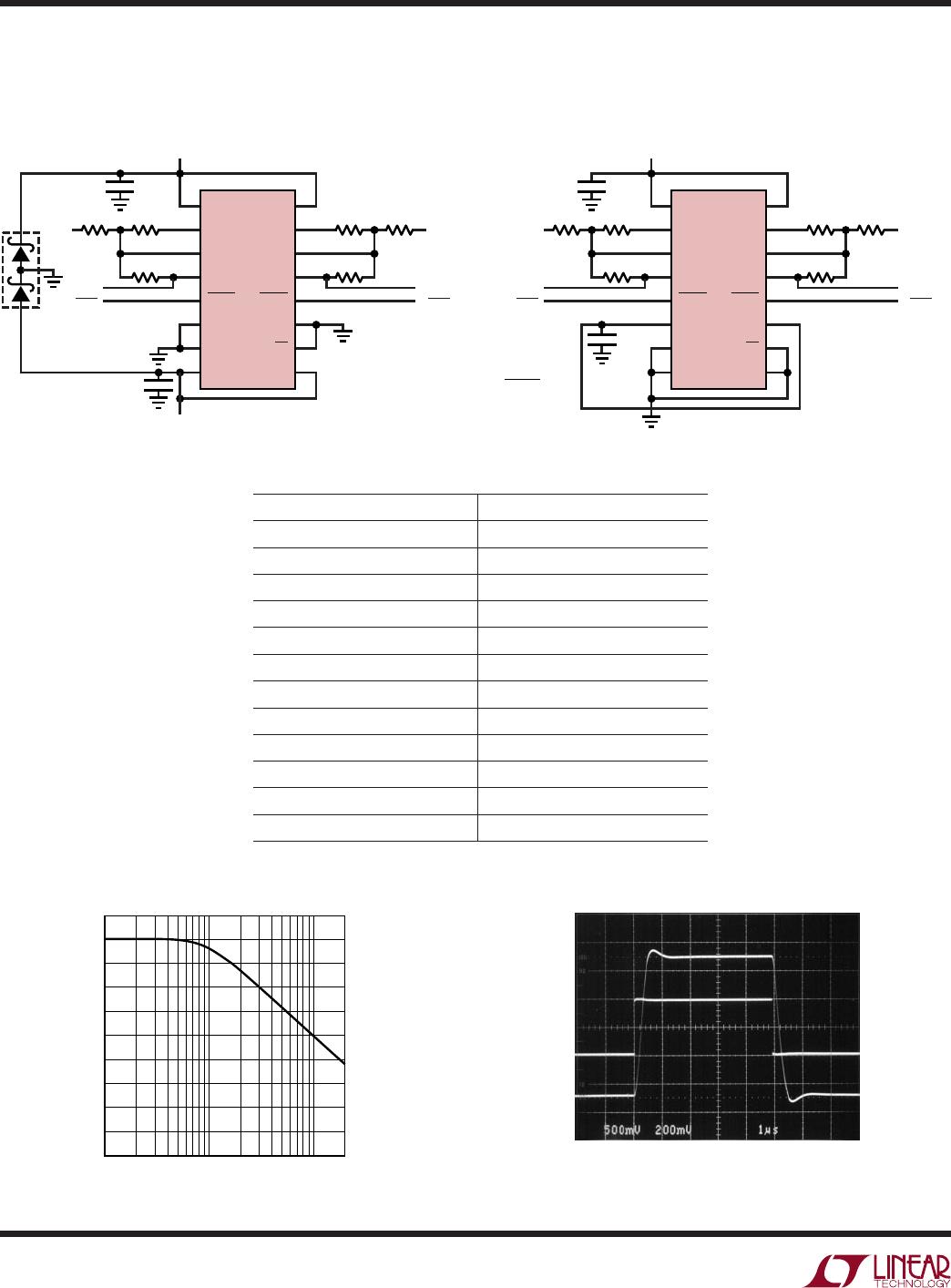
The following filter examples are provided to make it easy
to design a variety of filter stages. Both 2nd and 4th order
filters are shown. For each filer, a table of external resistor
values (standard 1% tolerance) is provided. These resistor
values have been adjusted to compensate for the finite
gain bandwidth product of the LT1568 amplifiers.
To implement a filter, simply connect the resistor values
shown in the table for the cutoff frequency desired. If the
desired cutoff frequency is not shown in the table of
values, use interpolation as recommended in the next
section.
DESIGNING FOR ANY CUTOFF FREQUENCY
To implement a lowpass filter with a cutoff frequency not
included in the design table, resistor values can be inter-
polated in the following manner:
For a Cutoff Frequency, f
C
, Less Than 1MHz
Start with the resistor values for f
C
= 1MHz and then scale
them up by the ratio of (1MHz/f
C
).
APPLICATIO S I FOR ATIO
WUUU
Example: Implement a 2nd order lowpass Chebyshev filter
with an f
C
of 256kHz. From Table 2 the values for f
C
of
1MHz are R11 = R21 = 976 and R31 825.
Scaling for f
C
= 256kHz:
R11 = R21 = 976 • (1MHz/256kHz) 3.83k
R31 = 825 • (1MHz/256kHz) 3.24k
For a Cutoff Frequency, f
C
, Between Values Given in a
Design Table
Start with the resistor values for the cutoff frequency
closest to the desired one and scale the values up or down
accordingly.
Example: Implement a 2nd order lowpass Chebyshev filter
with an f
C
of 3.2MHz. From Table 2 the closest values are
for f
C
of 3MHz and are R11 = R21 = 316 and R31 = 274.
Scaling for f
C
= 3.2MHz:
R11 = R21 = 316 • (3MHz/3.2MHz) 294
R31 = 274 • (3MHz/3.2MHz) 255
LT1568
12
1568f
Table 1. Resistor Values in Ohms, Dual 2nd Order
Butterworth, Gain = 1, R12 = R11, R22 = R21, R32 = R31
f
CUTOFF
(MHz) R11 = R21 = R31
0.2 6340
0.5 2550
1 1270
2 634
3 422
4 324
5 255
6 210
7 182
8 162
9 143
10 127
FREQUENCY (MHz)
0.1
–50
GAIN (dB)
–40
–30
–20
–10
11020
1568 TA07
–60
–70
–80
–90
0
10
Amplitude Response
2nd Order Butterworth, f
CUTOFF
= 1MHz
Transient Response
2nd Order Butterworth, f
CUTOFF
= 1MHz
INPUT
500mV/DIV
OUTPUT
200mV/DIV
1µs/DIV
1568 TA08
Dual 2nd Order Lowpass Filter,
Dual Supply Operation
1
2
3
4
5
6
7
8
16
15
14
13
12
11
10
9
V
+
INVA
SA
OUTA
OUTA
GNDA
NC
V
V
+
INVB
SB
OUTB
OUTB
GNDB
EN
V
0.1µF
BAT54S
V
IN1
V
OUTA
V
OUTA
V
IN2
V
OUTB
V
OUTB
R11 R31
R22
R32 R12
R21
0.1µF
–5V
1568 TA03
5V
LT1568
Dual 2nd Order Lowpass Filter,
Single Supply Operation
1
2
3
4
5
6
7
8
16
15
14
13
12
11
10
9
V
+
INVA
SA
OUTA
OUTA
GNDA
NC
V
V
+
INVB
SB
OUTB
OUTB
GNDB
EN
V
0.1µF
V
IN1
V
OUTA
V
OUTA
V
IN2
V
OUTB
V
OUTB
R11 R31
R22
R32 R12
R21
0.1µF
1568 TA04
2.7V V
+
10V
LT1568
R
ff
C CUTOFF
11=R21= R31=R = 128
10MHz
f
C
=
DUAL 2nd ORDER LOWPASS FILTER DESIG S
U

LT1568CGN#TRPBF

Mfr. #:
Manufacturer:
Analog Devices Inc.
Description:
Active Filter Very L N, Hi Freq Active RC, Filt Buildi
Lifecycle:
New from this manufacturer.
Delivery:
DHL FedEx Ups TNT EMS
Payment:
T/T Paypal Visa MoneyGram Western Union