Expand menu
Hello, Sign in
My Account
0
Cart
Home
Products
Sensors
Semiconductors
Passive Components
Connectors
Power
Electromechanical
Optoelectronics
Circuit Protection
Integrated Circuits - ICs
Main Products
Manufacturers
Blog
Services
About OMO
About Us
Contact Us
Check Stock
RP73D1J23R2BTG
P1-P3
P4-P6
P7-P9
P10-P10
SMD High Power Precision Resistors
1773272 CIS WR 09
/2015
Dimensions in
millimetres unless
otherwise specified
Dimensions Shown for
reference purposes only.
Specifications subject to
change
For Email, phone or live chat,
go to: www.te.com/help
Electrical Characteristic
s RP73
P series
–
High Power
0603
Rated Power
@ 70°C
0.166W
Resistan
ce
range Ω
Min
10R
10R
10R
Max
332K
332K
332K
Tolerance (
%)
0.1
0.5
1.0
Code Lett
er
B
D
F
TCR (PPM / °C)
25
50
25
50
25
50
Code Lett
er
F
G
F
G
F
G
Selectio
n series
E24 & E96
Max. operat
ing
voltage
100V
Max overl
oad voltage
150V
Operati
ng
temperatur
e range
-55 ~ +155°C
Insulation
resistance
>MΩ
Stability
0.5%
0805
Rated Power
@ 70°C
0.25W
Resistan
ce
range Ω
Min
10R
10R
10R
Max
499K
499K
499K
Tolerance (
%)
0.1
0.5
1.0
Code Lett
er
B
D
F
TCR (PPM / °C)
25
50
25
50
25
50
Code Lett
er
F
G
F
G
F
G
Selectio
n series
E24 & E96
Max. operat
ing
voltage
150V
Max overl
oad voltage
300V
Operati
ng
temperatur
e range
-55 ~ +155°C
Insulation
resistance
>MΩ
Stability
0.5%
1206
Rated Power
@ 70°C
0.33W
Resistan
ce
range Ω
Min
10R
10R
10R
Max
1M0
1M0
1M0
Tolerance (
%)
0.1
0.5
1.0
Code Lett
er
B
D
F
TCR (PPM / °C)
25
50
25
50
25
50
Code Lett
er
F
G
F
G
F
G
Selectio
n series
E24 & E96
Max. operat
ing
voltage
200V
Max overl
oad voltage
400V
Operati
ng
temperatur
e range
-55 ~ +155°C
Insulation
resistance
>MΩ
Stability
0.5%
Operating Voltage=
√P*R or
Max. operating
oltage listed aoe, hih
eer is lo
er.
Oerload Voltage=.
*√P*
R or Max. oerload
oltage listed
aoe, hihe
er is loer.
SMD High Power Precision Resistors
1773272 CIS WR 09
/2015
Dimensions in
millimetres unless
otherwise specified
Dimensions Shown for
reference purposes only.
Specifications subject to
change
For Email, phone or live chat,
go to: www.te.com/help
Environmental Characteristics
Item
Require
ment
Test Metho
d
Tol. ≤.%
TOL. >0.05%
Temperature Coe
fficient
of Resi
stance (TCR)
As per TCRs spe
cified in Ele
ctrical Characte
ristics
tables
MIL-STD-202 Metho
d 304
+25/-55/+25/+125/+25°
C
Short Time Ove
rload
ΔR±0.2%
ΔR±0.2%
JIS-C-5201-1 5.5
RCWV*2.5 or Max. ove
rload vo
ltage
whichever
is lower for 5 se
conds
Insulation
Resistance
> MΩ
MIL-STD-202 Metho
d 302
Apply 100VDC for
1 minute
Endurance
ΔR±0.5%
MIL-STD-202 Metho
d 108A
70±2°C, RCWV fo
r 1000 hrs wit
h 1.5 hrs
ON and .
hrs
OFF
Damp Heat with Lo
ad
ΔR±.
5%
ΔR±.
%
MIL-STD-202 Metho
d 103B
40±2°C, 90~95% R
.H. RCWV for 1000
hrs
with 1.5
hrs O
N and . hrs O
FF
Bending Stre
ngth
ΔR±.%
ΔR±.%
JIS-C-5201-1 6.1.4
Bending amplit
ude 3 mm for 10 se
conds
Solderabil
ity
95% min. coverage
MIL-STD-202 Metho
d 208H
245±5°C for 3 sec
onds
Resistan
ce to Soldering
Heat
ΔR±.%
ΔR±.%
MIL-STD-202 Metho
d 210E
260±5°C for 10 sec
onds
Dielectri
c Withstand
Voltage
By Type
MIL-STD-202 Metho
d 301
Max. overlo
ad voltage for
1 minute
Thermal Shock
ΔR±.%
ΔR±.%
MIL-STD-202 Metho
d 107G
-55°C ~150°C, 100 c
ycles
Low Temperatur
e
Operati
on
ΔR±.
5%
ΔR±.
%
JIS-C-5201-1 7.1
1 hour, -65°C, fol
lowed by 45 minu
tes of
RCWV
Storage Tempera
ture: 25±3°C; Hu
midity < 80
%RH
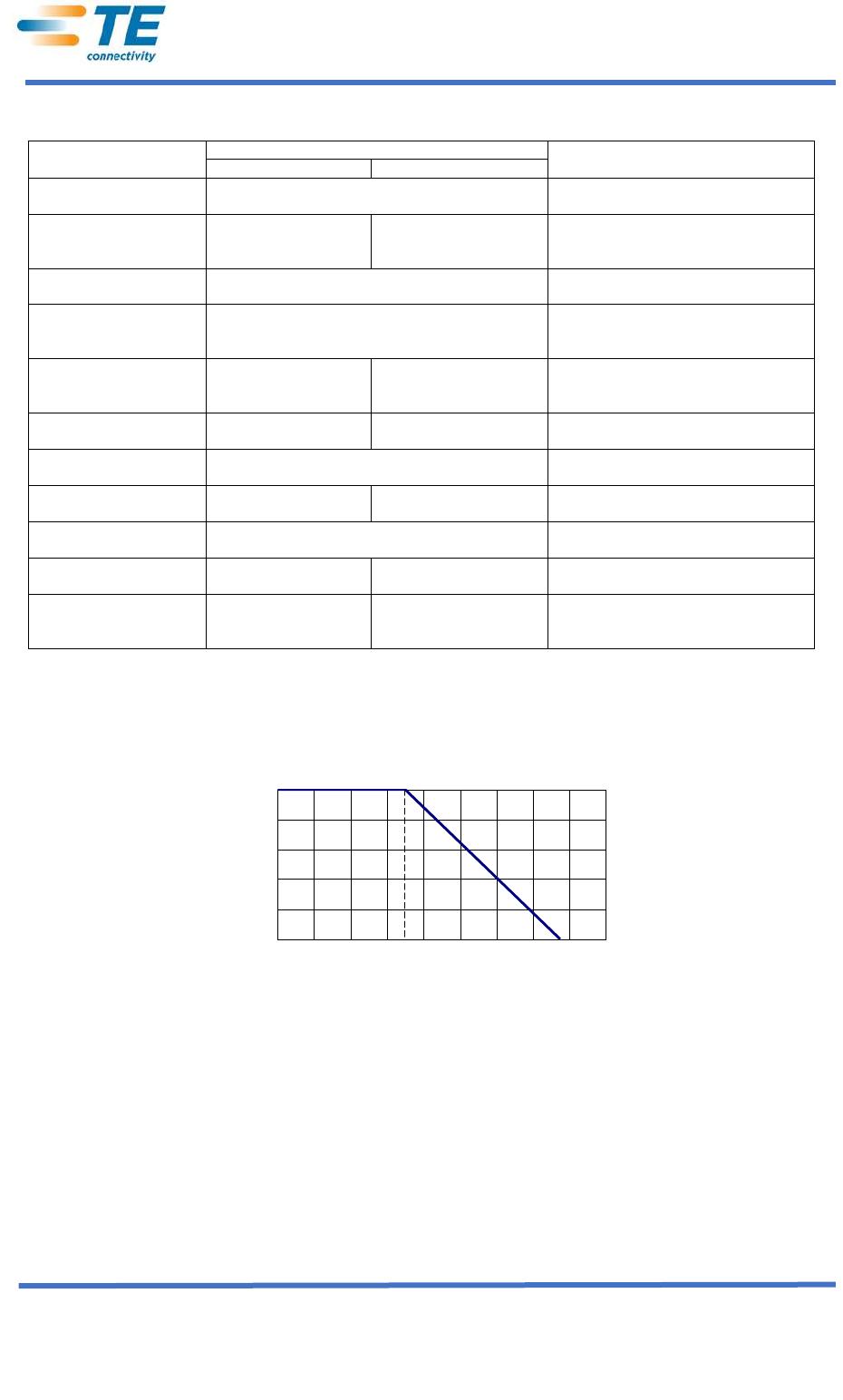
Derating Curve
For resistors operated in ambient temperatures above 70°C, power rating
must be derated in accordance with this
curve
0
20
40
60
80
100
0
20
40
60
80
100
120
140
160
180
Ambie
n
t
T
em
perat
u
re(
℃
)
Pow
er
rat
i
o(%)
SMD High Power Precision Resistors
1773272 CIS WR 09
/2015
Dimensions in
millimetres unless
otherwise specified
Dimensions Shown for
reference purposes only.
Specifications subject to
change
For Email, phone or live chat,
go to: www.te.com/help
Construction and di
mensions
Alumina Substrate
Edge Electrod
e (NiCr)
Resistor Layer
(NiCr)
Bottom Electrode
(Ag)
Barrier Layer
(Ni)
Overcoat (Epox
y)
Top Electrode (
Ag)
External Electro
de (Sn)
Marking
Size
L (mm)
W (mm)
T (mm)
D1 (mm)
D2 (mm)
Weight (g)
(1000 Pcs.)
0402
1.00±0.05
0.50±0.05
0.30±0.05
0.20±0.10
0.20±0.10
0.54
0603
1.55±0.10
0.80±0.10
0.45±0.10
0.30±0.20
0.30±0.20
1.83
0805
2.00±0.15
1.25±0.15
0.55±0.10
0.30±0.20
0.40±0.20
4.71
1206
3.05±0.15
1.55±0.15
0.55±0.10
0.42±0.20
0.35±0.25
9.02
1210
3.10±0.15
2.40±0.15
0.55±0.10
0.40±0.20
0.55±0.25
10
2010
4.90±0.15
2.40±0.15
0.55±0.10
0.60±0.30
0.50±0.25
23.61
2512
6.30±0.15
3.10±0.15
0.55±0.10
0.60±0.30
0.50±0.25
38.06
Suggested PCB La
yout Plan
Recommended La
nd Pattern
Size
A
B
C
0402
0.50
0.50
0.60±0.2
0603
0.80
1.00
0.90±0.2
0805
1.00
1.00
1.35±0.2
1206
2.00
1.15
1.70±0.2
1210
2.00
1.15
2.50±0.2
2010
3.60
1.40
2.50±0.2
2512
4.90
1.60
3.10±0.2
L
T
D1
D2
W
P1-P3
P4-P6
P7-P9
P10-P10
RP73D1J23R2BTG
Mfr. #:
Buy RP73D1J23R2BTG
Manufacturer:
Description:
Thin Film Resistors - SMD RP 1J 23R2 0.1% 15PPM CUT LENGTH
Lifecycle:
New from this manufacturer.
Delivery:
DHL
FedEx
Ups
TNT
EMS
Payment:
T/T
Paypal
Visa
MoneyGram
Western
Union
Products related to this Datasheet
RP73D1J6K65BTG
RP73D1J25K5BTG
RP73D1J332RBTG
RP73D1J665RBTG
RP73PF1J562RBTDF
RP73D1J182KBTG
RP73D1J169RBTG
RP73PF1J127RBTDF
RP73D1J23R2BTG
RP73D1J681RBTG
RP73D1J34R8BTG
RP73D1J7K87BTG
RP73D1J1K87BTG
RP73D1J3K48BTG
RP73D1J4K42BTG
RP73D1J48K7BTG
RP73D1J619RBTG
RP73D1J4R99BTG
RP73D1J340RBTG
RP73D1J5R36BTG
RP73D1J90R9BTG
RP73D1J10K2BTG
RP73D1J887RBTG
RP73PF1J2K1BTDF
RP73D1J221KBTG
RP73D1J21R5BTG
RP73D1J8R66BTG
RP73D1J412RBTG
RP73D1J3K16BTG
RP73D1J750RBTG
RP73D1J178KBTG
RP73D1J2K55BTG
RP73D1J374RBTG
RP73D1J6R98BTG
RP73D1J383RBTG
RP73D1J2K37BTG