7
FN8179.2
December 21, 2009
DC Electrical Specifications (Over recommended operating conditions unless otherwise specified.
SYMBOL PARAMETER TEST CONDITIONS
LIMITS
UNIT
MIN
(Note 9)
TYP
(Note 8)
MAX
(Note 9)
V
CC
Supply Voltage X9315 4.5 5.5 V
X9315-2.7 2.7 5.5 V
I
CC1
V
CC
active current (Increment) CS = V
IL
, U/D = V
IL
or V
IH
and INC = 0.4V
@ max. t
CYC
80 µA
I
CC2
V
CC
active current (Store) (EEPROM
Store)
CS = V
IH
, U/D = V
IL
or V
IH
and INC = V
IH
@
max. t
WR
400 µA
I
SB
Standby supply current CS = V
CC
- 0.3V, U/D and INC = V
SS
or V
CC
- 0.3V
A
I
LI
CS, INC, U/D input leakage current V
IN
= V
SS
to V
CC
-10 +10 µA
V
IH
CS, INC, U/D input HIGH voltage V
CC
x 0.7 V
CC
+ 0.5 V
V
IL
CS, INC, U/D input LOW voltage -0.5 V
CC
x 0.1 V
C
IN
CS, INC, U/D input capacitance V
CC
= 5V, V
IN
= V
SS
, T
A
= +25°C, f = 1MHz 10 pF
Endurance and Data Retention
PARAMETER MIN UNIT
Minimum endurance 100,000 Data changes per bit
Data retention 100 Years
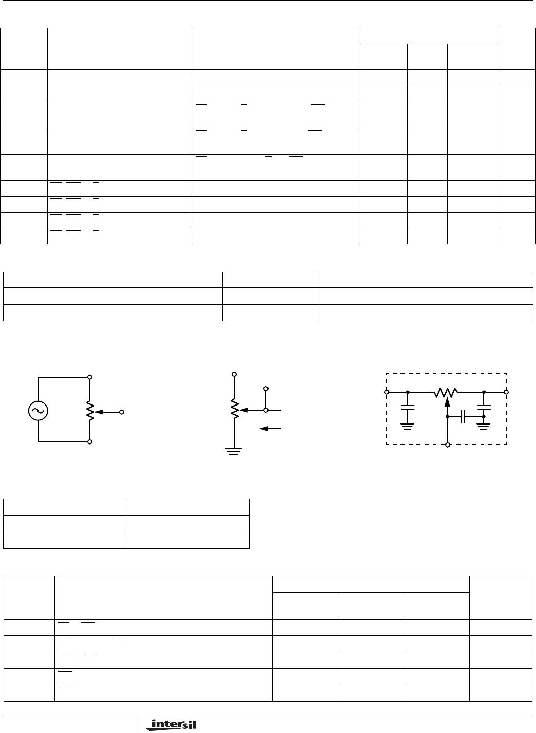
Test Circuit #1 Test Circuit #2 Circuit #3 SPICE Macro Model
Test Point
V
W
/R
W
V
H
/R
H
V
L
/R
L
V
S
Force
Current
V
L
VW
Test Point
V
H
/R
H
V
W
/R
W
V
L
/R
L
C
H
C
L
R
W
10pF
10pF
R
H
R
L
R
TOTAL
C
W
25pF
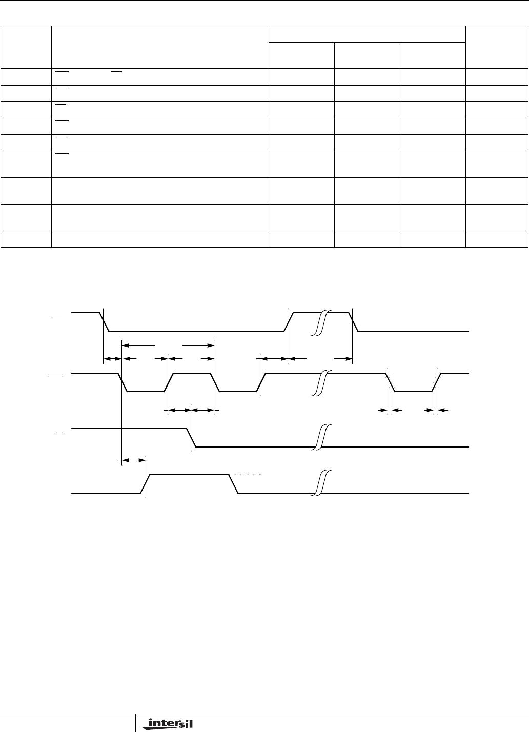
AC Conditions of Test
Input pulse levels 0V to 3V
Input rise and fall times 10ns
Input reference levels 1.5V
AC Electrical Specifications (Over recommended operating conditions unless otherwise specified)
SYMBOL PARAMETER
LIMITS
UNIT
MIN
(Note 9)
TYP
(Note 8)
MAX
(Note 9)
t
Cl
CS to INC setup 100 ns
t
lD
INC HIGH to U/D change 100 ns
t
DI
U/D to INC setup 2.9 µs
t
lL
INC LOW period 1 µs
t
lH
INC HIGH period 1 µs
X9315
8
FN8179.2
December 21, 2009
AC Timing
NOTE:
11. MI in the A.C. timing diagram refers to the minimum incremental change in the V
W
output due to a change in the wiper position.
t
lC
INC Inactive to CS inactive 1 µs
t
CPH
CS Deselect time (NO STORE) 100 ns
t
CPH
CS Deselect time (STORE) 10 ms
t
IW
INC to Vw change 1 5 µs
t
CYC
INC cycle time 4 µs
t
R,
t
F
(Note 10)
INC
input rise and fall time 500 µs
t
PU
(Note 10)
Power-up to wiper stable s
t
R
V
CC
(Note 10)
V
CC
power-up rate 0.2 50 V/ms
t
WR
Store cycle 510ms
NOTE:
10. This parameter is not 100% tested.
AC Electrical Specifications (Over recommended operating conditions unless otherwise specified) (Continued)
SYMBOL PARAMETER
LIMITS
UNIT
MIN
(Note 9)
TYP
(Note 8)
MAX
(Note 9)
CS
INC
U/D
V
W
t
CI
t
IL
t
IH
t
CYC
t
ID DI
t
IW
MI
(Note 9)
t
IC
t
CPH
t
F
t
R
10%
90% 90%
(Store)
X9315
9
FN8179.2
December 21, 2009
Symbol Table
Performance Characteristics (Typical)
Typical Noise
WAVEFORM INPUTS OUTPUTS
Must be
steady
Will be
steady
May change
from Low to
High
Will change
from Low to
High
May change
from High to
Low
Will change
from High to
Low
Don’t Care:
Changes
Allowed
Changing:
State Not
Known
N/A Center Line
is High
Impedance
0
-10
-20
-30
-40
-50
-60
-70
-80
-90
-100
-110
-120
-130
-140
-150
0 102030405060708090100
Frequency (kHz)
Noise (dB)
110 120 130 140 150 160 170 180 190 200
X9315

X9315UMZ-2.7T1

Mfr. #:
Manufacturer:
Renesas / Intersil
Description:
Digital Potentiometer ICs CMOS XDCP 50KOHM 32 TAPS 8LD
Lifecycle:
New from this manufacturer.
Delivery:
DHL FedEx Ups TNT EMS
Payment:
T/T Paypal Visa MoneyGram Western Union