AP8020JLL
050-7079 Rev B 7-2004
I
D
(A) I
D
(A)
FIGURE 14, DELAY TIMES vs CURRENT FIGURE 15, RISE AND FALL TIMES vs CURRENT
I
D
(A) R
G
, GATE RESISTANCE (Ohms)
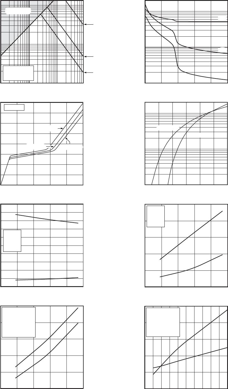
FIGURE 16, SWITCHING ENERGY vs CURRENT FIGURE 17, SWITCHING ENERGY VS. GATE RESISTANCE
V
DD
= 533V
R
G
= 5Ω
T
J
= 125°C
L = 100µH
t
r
t
f
SWITCHING ENERGY (µJ) t
d(on)
and t
d(off)
(ns)
SWITCHING ENERGY (µJ) t
r
and t
f
(ns)
10 20 30 40 50 60 10 20 30 40 50 60
10 20 30 40 50 60 0 5 10 15 20 25 30 35 40 45 50
t
d(on)
t
d(off)
E
on
E
off
200
180
160
140
120
100
80
60
40
20
0
2500
2000
1500
1000
500
0
V
DD
= 533V
R
G
= 5Ω
T
J
= 125°C
L = 100µH
V
DD
= 533V
R
G
= 5Ω
T
J
= 125°C
L = 100µH
E
ON
includes
diode reverse recovery.
V
DS
, DRAIN-TO-SOURCE VOLTAGE (VOLTS) V
DS
, DRAIN-TO-SOURCE VOLTAGE (VOLTS)
FIGURE 10, MAXIMUM SAFE OPERATING AREA FIGURE 11, CAPACITANCE vs DRAIN-TO-SOURCE VOLTAGE
Q
g
, TOTAL GATE CHARGE (nC) V
SD
, SOURCE-TO-DRAIN VOLTAGE (VOLTS)
FIGURE 12, GATE CHARGES vs GATE-TO-SOURCE VOLTAGE FIGURE 13, SOURCE-DRAIN DIODE FORWARD VOLTAGE
V
GS
, GATE-TO-SOURCE VOLTAGE (VOLTS) I
D
, DRAIN CURRENT (AMPERES)
I
DR
, REVERSE DRAIN CURRENT (AMPERES) C, CAPACITANCE (pF)
1 10 100 800 0 10 20 30 40 50
0 50 100 150 200 250 0.3 0.5 0.7 0.9 1.1 1.3 1.5
132
100
50
10
1
16
12
8
4
0
20,000
10,000
1,000
100
200
100
10
1
C
rss
C
iss
C
oss
T
J
=+150°C
T
J
=+25°C
V
DS
=400V
V
DS
=160V
V
DS
=640V
I
D
= 33A
T
C
=+25°C
T
J
=+150°C
SINGLE PULSE
OPERATION HERE
LIMITED BY R
DS
(ON)
10mS
1mS
100µS
100
80
60
40
20
0
5000
4000
3000
2000
1000
0
E
on
E
off
V
DD
= 533V
I
D
= 38A
T
J
= 125°C
L = 100µH
E
ON
includes
diode reverse recovery.
