TL431, A, B Series, NCV431A, B
http://onsemi.com
4
ELECTRICAL CHARACTERISTICS (T
A
= 25°C, unless otherwise noted.)
Characteristic
Symbol
TL431AI / NCV431AI TL431AC
TL431BI / TL431BV
NCV431BV
Unit
Min Typ Max Min Typ Max Min Typ Max
Reference Input Voltage (Figure 1)
V
KA
= V
ref
, I
K
= 10 mA
T
A
= 25°C
T
A
= T
low
to T
high
V
ref
2.47
2.44
2.495
−
2.52
2.55
2.47
2.453
2.495
−
2.52
2.537
2.485
2.475
2.495
2.495
2.505
2.515
V
Reference Input Voltage Deviation Over
Temperature Range (Figure 1, Notes 4, 5)
V
KA
= V
ref,
I
K
= 10 mA
DV
ref
− 7.0 30 − 3.0 17 − 3.0 17 mV
Ratio of Change in Reference Input Voltage to
Change in Cathode to Anode Voltage
I
K
= 10 mA (Figure 2),
DV
KA
= 10 V to V
ref
DV
KA
= 36 V to 10 V
DV
ref
DV
KA
−
−
−1.4
−1.0
−2.7
−2.0
−
−
−1.4
−1.0
−2.7
−2.0
−
−
−1.4
−1.0
−2.7
−2.0
mV/V
Reference Input Current (Figure 2)
I
K
= 10 mA, R1 = 10 k, R2 = ∞
T
A
= 25°C
T
A
= T
low
to T
high
(Note 4)
I
ref
−
−
1.8
−
4.0
6.5
−
−
1.8
−
4.0
5.2
−
−
1.1
−
2.0
4.0
mA
Reference Input Current Deviation Over
Temperature Range (Figure 2, Note 4)
I
K
= 10 mA, R1 = 10 k, R2 = ∞
DI
ref
− 0.8 2.5 − 0.4 1.2 − 0.8 2.5
mA
Minimum Cathode Current For Regulation
V
KA
= V
ref
(Figure 1)
I
min
− 0.5 1.0 − 0.5 1.0 − 0.5 1.0 mA
Off−State Cathode Current (Figure 3)
V
KA
= 36 V, V
ref
= 0 V
I
off
− 20 1000 − 20 1000 − 0.23 500 nA
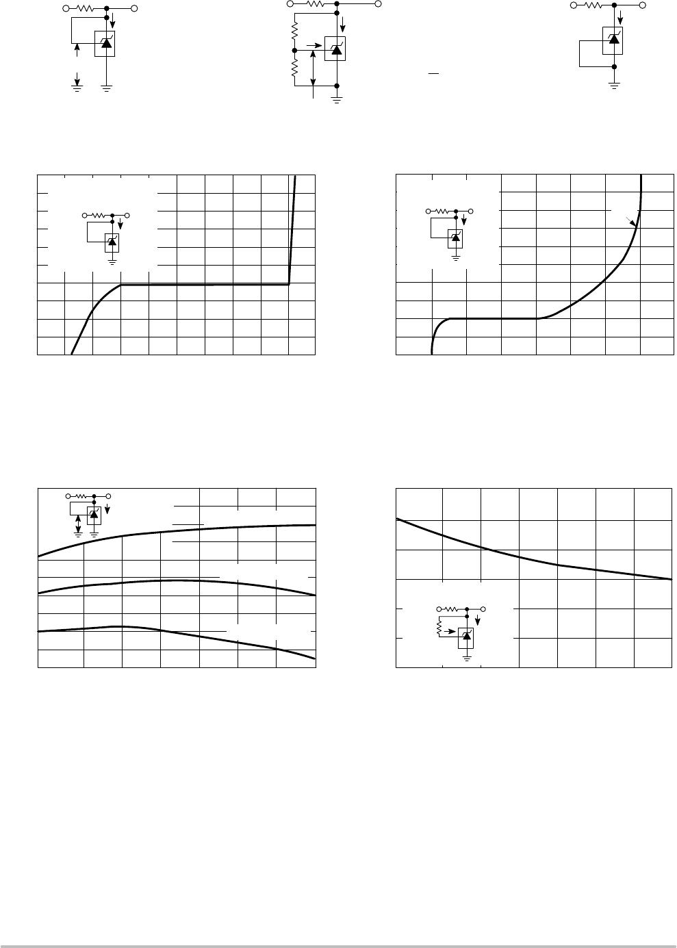
Dynamic Impedance (Figure 1, Note 6)
V
KA
= V
ref
, DI
K
= 1.0 mA to 100 mA
f ≤ 1.0 kHz
|Z
KA
| − 0.22 0.5 − 0.22 0.5 − 0.14 0.3
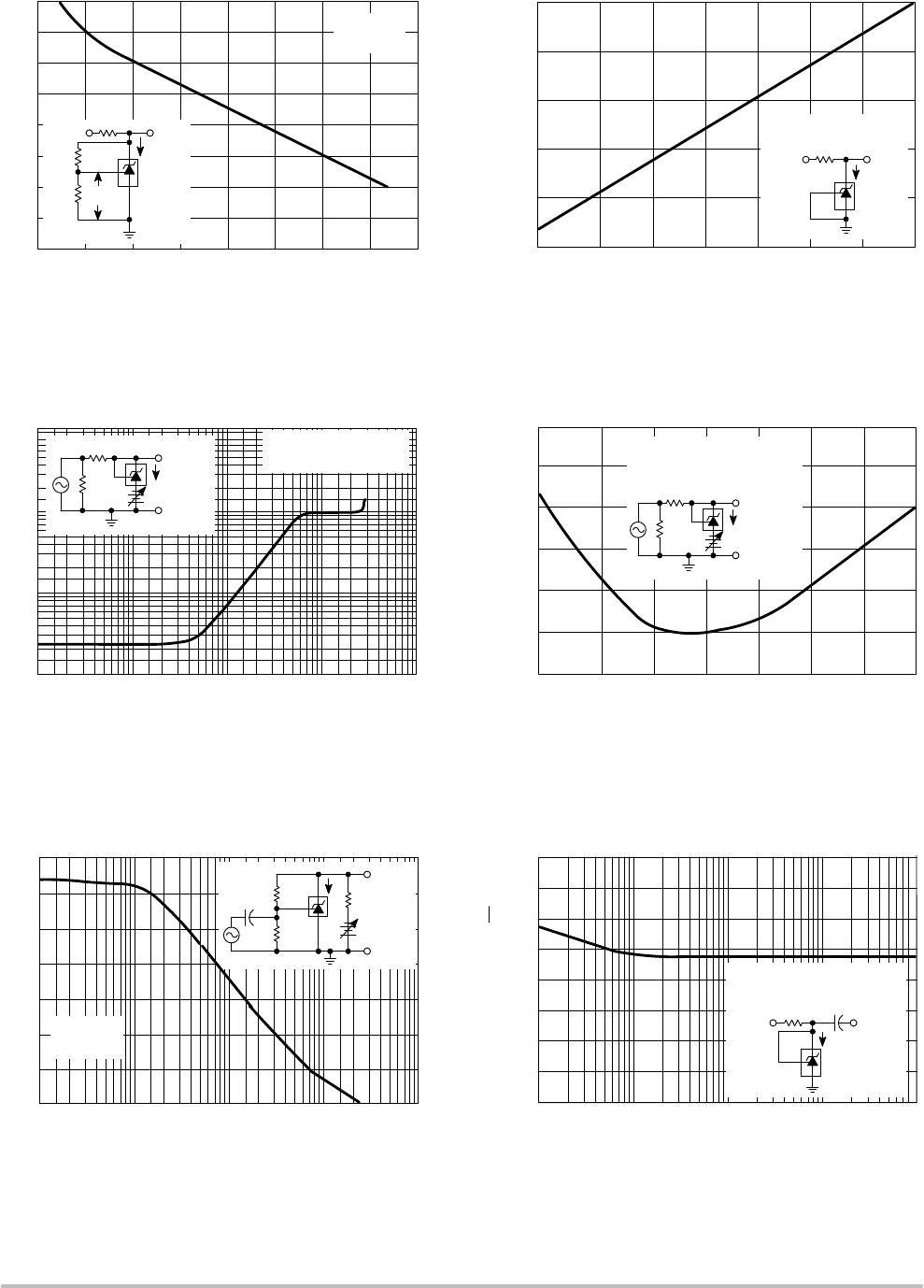
W
4. T
low
= −40°C for TL431AIP TL431AILP, TL431IP, TL431ILP, TL431BID, TL431BIP, TL431BILP, TL431BV, TL431AIDM, TL431IDM,
TL431BIDM, NCV431AIDMR2, NCV431AIDR2
=0°C for TL431ACP, TL431ACLP, TL431CP, TL431CLP, TL431CD, TL431ACD, TL431BCD, TL431BCP, TL431BCLP, TL431CDM,
TL431ACDM, TL431BCDM
T
high
= +85°C for TL431AIP, TL431AILP, TL431IP, TL431ILP, TL431BID, TL431BIP, TL431BILP, TL431IDM, TL431AIDM, TL431BIDM
= +70°C for TL431ACP, TL431ACLP, TL431CP, TL431ACD, TL431BCD, TL431BCP, TL431BCLP, TL431CDM, TL431ACDM,
TL431BCDM
= +125°C TL431BV, NCV431AIDMR2, NCV431AIDR2, NCV431BVDMR2G
5. The deviation parameter DV
ref
is defined as the difference between the maximum and minimum values obtained over the full operating
ambient temperature range that applies.
DV
ref
= V
ref
max
-V
ref
min
DT
A
= T
2
- T
1
T2
Ambient Temperature
T1
V
ref
min
V
ref
max
The average temperature coefficient of the reference input voltage, aV
ref
is defined as:
V
ref
ppm
_C
+
ǒ
D V
ref
V
ref
@25_C
Ǔ
X10
6
D T
A
+
D V
ref
x10
6
D T
A
(V
ref
@25_C)
aV
ref
can be positive or negative depending on whether V
ref
Min or V
ref
Max occurs at the lower ambient temperature. (Refer to Figure 6.)
Example : DV
ref
+ 8.0 mV and slope is positive,
V
ref
@25_C + 2.495 V, DT
A
+ 70_C
a V
ref
+
0.008 x 10
6
70 (2.495)
+ 45.8 ppmń_C
6. The dynamic impedance Z
KA
is defined as
|Z
KA
| +
D V
KA
D I
K
When the device is programmed with two external resistors, R1 and R2, (refer
to Figure 2) the total dynamic impedance of the circuit is defined as:
|Z
KA
Ȁ| [ |Z
KA
|
ǒ
1 )
R1
R2
Ǔ
7. NCV431AIDMR2, NCV431AIDR2, NCV431BVDMR2G T
low
= −40°C, T
high
= +125°C. Guaranteed by design. NCV prefix is for automotive
and other applications requiring site and change control.