• All specifi cations are subject to change without notice.
Series Name
Dimensions L x W (mm)
Temperature Characteristics
Rated Voltage (DC)
Nominal Capacitance (pF)
Capacitance Tolerance
Packaging Style
Nominal Thickness
Code Length Width Terminal
1
0.60 ± 0.03 0.30 ± 0.03
0.10 min.
2
1.00 ± 0.05 0.50 ± 0.05
0.10 min.
3
1.60 ± 0.10 0.80 ± 0.10
0.20 min.
4
2.00 ± 0.20 1.25 ± 0.20
0.20 min.
5
3.20 ± 0.20 1.60 ± 0.20
0.20 min.
6
3.20 ± 0.40 2.50 ± 0.30
0.20 min.
8
4.50 ±0.40 3.20 ±0.40
0.20 min.
9
5.70 ±0.40 5.00 ±0.40
0.20 min.
*Dimension tolerance are typical values
Code Voltage (DC)
0J 6.3V
1A 10V
1C 16V
1E 25V
1V 35V
1H 50V
Code Tolerance
C
± 0.25pF
D
±0.50pF
J
±5%
K
±10%
M
±20%
Code Style
A 178 mm Reel, 4 mm Pitch
B 178 mm Reel, 2 mm Pitch
K 178 mm Reel, 8 mm Pitch
Temperature
Characteristics
Temperature Coefficient or
Capacitance Change
Temperature
Range
C0G
0±30 ppm/°C -55 to +125°C
X5R
±15% -55 to + 85°C
X7R
±15% -55 to +125°C
X7S
±22% -55 to +125°C
Ex. 0R2 = 0.2pF; 103 = 10,000pF; 105 = 1,000,000pF = 1,000nF = 1ȝF
CGA • 6 • P • 1 • X7S • 0J • 476 • M • 250 • A • C
Code Thickness
050 0.50 mm
030 0.30 mm
060 0.60 mm
125 1.25 mm
*See Thickness T Code for complete list
Special Reserved Code
Code Description
A, B TDK Internal Code
Code Thickness
A0.30 mm
B0.50 mm
C0.60 mm
E0.80 mm
F0.85 mm
H1.15 mm
J1.25 mm
L1.60 mm
M2.00 mm
N2.30 mm
P2.50 mm
Q2.80 mm
R3.20 mm
Thickness T Code (mm)
Symbol Condition
1
1 × R.V.
2
2 × R.V.
3
1.5 × R.V.
Voltage Condition
for Life Test
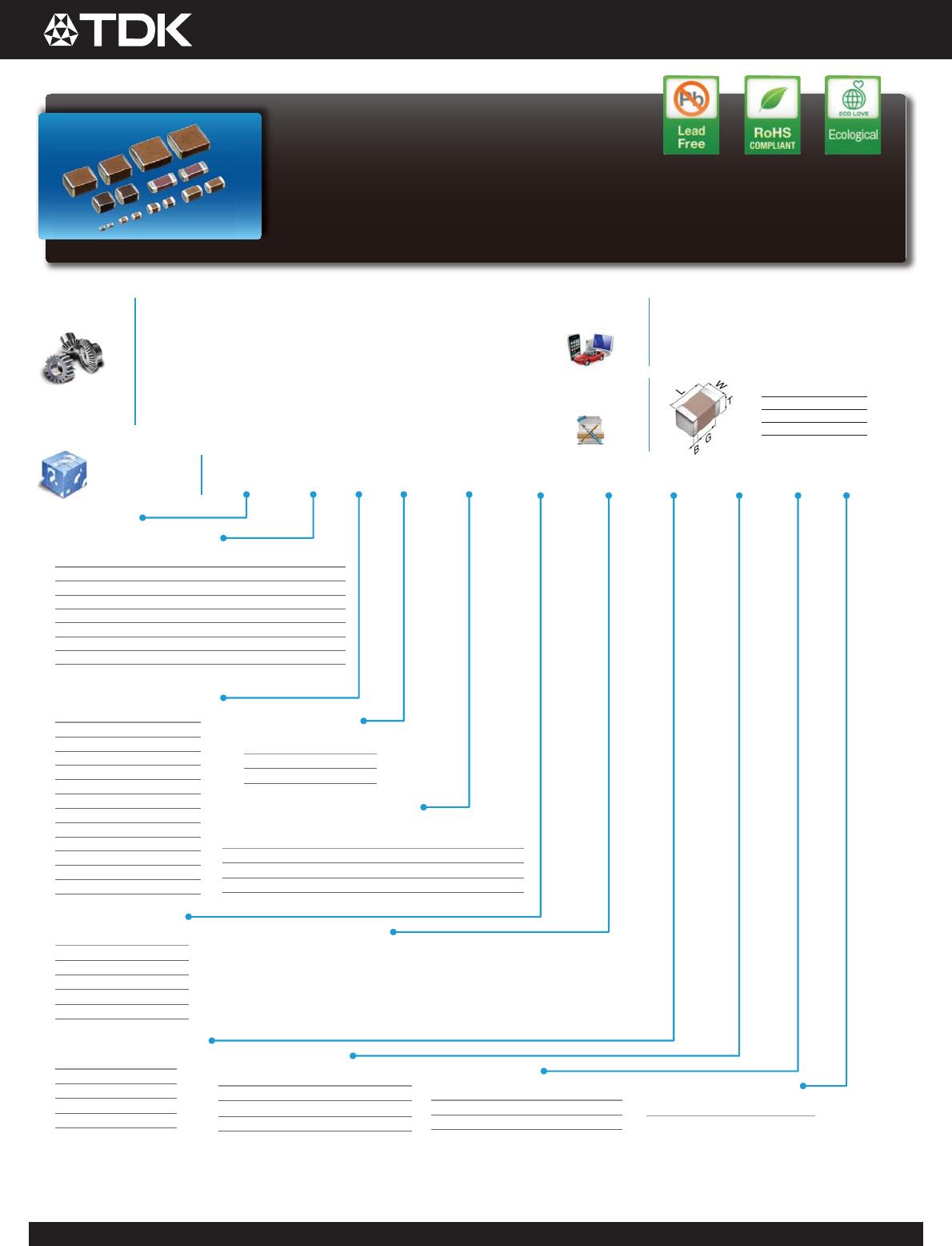
CGA Series
General (Up to 50V)
Type: CGA1 [EIA CC0201], CGA2 [EIA CC0402], CGA3 [EIA CC0603],
CGA4 [EIA CC0805], CGA5 [EIA CC1206], CGA6 [EIA CC1210], CGA8 [EIA CC1812],
CGA9 [EIA CC2220]
• Automotive engine control units
• Automotive sensor modules
• Automotive battery line smoothing
• Applications requiring higher reliability
• Switching power supply smoothing
Features Applications
L Body Length
W Body Width
T Body Height
B Terminal Width
G Terminal Spacing
Shape &
Dimensions
• High capacitance has been achieved through precision technologies
that enable the use of multiple thinner ceramic dielectric layers.
• A monolithic structure ensures superior mechanical strength and
reliability.
• Low ESL and excellent frequency characteristics allow for a circuit
design that closely conforms to theoretical values.
• Low self-heating and high ripple resistance due to low ESR.
• AEC-Q200 compliant.
The capacitance is expressed in three digit codes and in units of pico
Farads (pF). The first and second digits identify the first and second
significant figures of the capacitance. The third digit identifies the
multiplier. R designates a decimal point.
Catalog Number
Construction
Page 2
MULTILAYER CERAMIC CHIP CAPACITORS
20141219 / mlcc_automotive_general_en