14
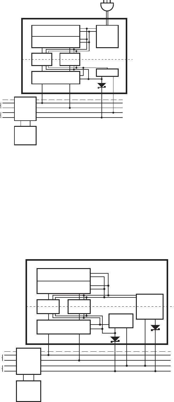
Figure 20. Isolated node with transceiver powered by the network
Isolated Node with Transceiver Powered by the Network
Figure 20 shows a node powered by both the network
and another source. In this case, the trans ceiver and
isolated (network) side of the two optocouplers are
powered by the network. The rest of the node is
powered by the AC line which is very benecial when
an application requires a signicant amount of power.
This method is also desirable as it does not heavily load
the network.
More importantly, the unique “dual-inverting” design
of the HCPL-x710 ensure the network will not “lock-up”
if either AC line power to the node is lost or the node
powered-o. Specically, when input power (V
DD1
) to
the HCPL-x710 located in the transmit path is eliminat-
ed, a RECESSIVE bus state is ensured as the HCPL-x710
output voltage (V
O
) go HIGH.
*Bus V+ Sensing
It is suggested that the Bus V+ sense block shown in
Figure 20 be implemented. A locally powered node
with an un-powered isolated Physical Layer will ac-
cumulate errors and become bus-o if it attempts to
transmit. The Bus V+ sense signal would be used to
change the BOI attribute of the DeviceNet Object to the
“auto-reset” (01) value. Refer to Volume 1, Section 5.5.3.
This would cause the node to continually reset until bus
power was detected. Once power was detected, the
BOI attribute would be returned to the “hold in bus-o”
(00) value. The BOI attribute should not be left in the
“auto-reset” (01) value since this defeats the jabber pro-
tection capability of the CAN error connement. Any in-
expensive low frequency optical isolator can be used to
implement this feature.
NODE/APP SPECIFIC
µP/CAN
HCPL
0710
HCPL
0710
TRANSCEIVER
NON ISO
5 V
REG.
NETWORK
POWER
SUPPLY
V+ (SIGNAL)
V– (SIGNAL)
V+ (POWER)
V– (POWER)
GALVANIC
ISOLATION
BOUNDARY
AC LINE
DRAIN/SHIELD
SIGNAL
POWER
HCPL
0710
* OPTIONAL FOR BUS V + SENSE