DMN2100UDM-7

DMN2100UDM
Document number: DS31186 Rev. 5 - 2
1 of 6
www.diodes.com
May 2012
© Diodes Incorporated
DMN2100UDM
NEW PRODUCT
N-CHANNEL ENHANCEMENT MODE MOSFET
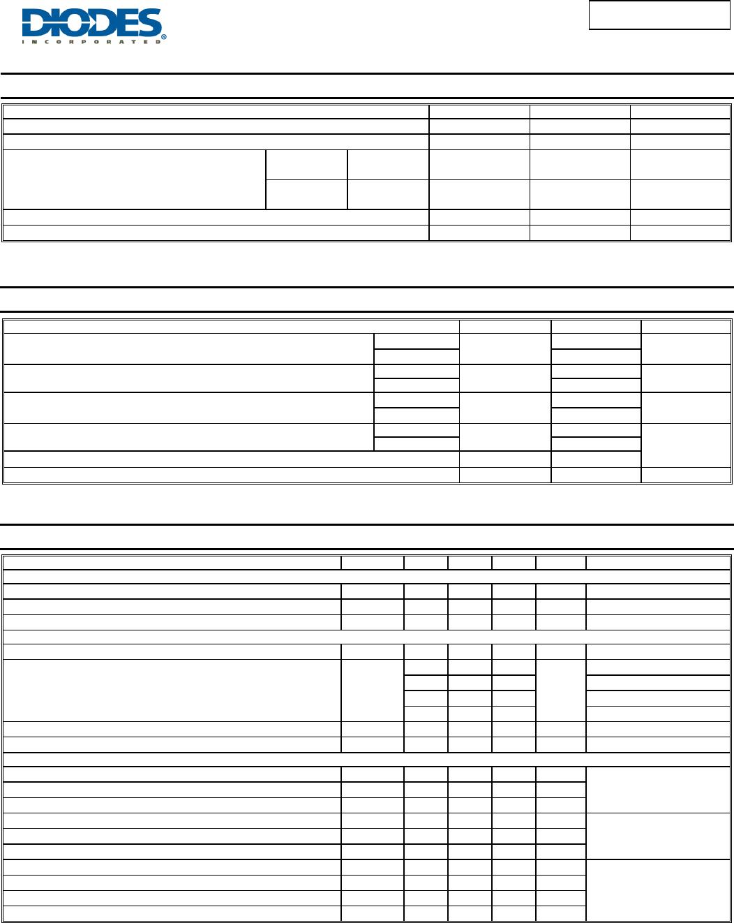
Product Summary
V
(BR)DSS
R
DS(ON)
max
I
D
max
T
A
= 25°C
20V
55mΩ @ V
GS
= 4.5V
4.0A
70m @ V
GS
= 2.5V
3.5A
90m @ V
GS
= 1.8V
3.1A
130m @ V
GS
= 1.5V
2.5A
Features and Benefits
Low On-Resistance
Low Gate Threshold Voltage
Low Input Capacitance
Fast Switching Speed
ESD Protected Gate
Totally Lead-Free & Fully RoHS Compliant (Notes 1 & 2)
Halogen and Antimony Free. “Green” Device (Note 3)
Qualified to AEC-Q101 Standards for High Reliability
Description and Applications
This new generation MOSFET has been designed to minimize the on-
state resistance (R
DS(on)
) and yet maintain superior switching
performance, making it ideal for high efficiency power management
applications.
General Purpose Interfacing Switch
Power Management Functions
Mechanical Data
Case: SOT26
Case Material: Molded Plastic, “Green” Molding Compound.
UL Flammability Classification Rating 94V-0
Moisture Sensitivity: Level 1 per J-STD-020
Terminal Connections: See Diagram
Terminals: Finish Matte Tin annealed over Copper leadframe.
Solderable per MIL-STD-202, Method 208
Weight: 0.015 grams (approximate)
Ordering Information (Note 4)
Part Number Case Packaging
DMN2100UDM-7 SOT26 3000/Tape & Reel
Notes: 1. No purposely added lead. Fully EU Directive 2002/95/EC (RoHS) & 2011/65/EU (RoHS 2) compliant.
2. See http://www.diodes.com for more information about Diodes Incorporated’s definitions of Halogen- and Antimony-free, "Green" and Lead-free.
3. Halogen- and Antimony-free "Green” products are defined as those which contain <900ppm bromine, <900ppm chlorine (<1500ppm total Br + Cl) and
<1000ppm antimony compounds.
4. For packaging details, go to our website at http://www.diodes.com..
Marking Information
Date Code Key
Year 2007 2008 2009 2010 2011 2012 2013 2014 2015 2016 2017
Code U V W X Y Z A B C D E
Month Jan Feb Mar Apr May Jun Jul Aug Sep Oct Nov Dec
Code 1 2 3 4 5 6 7 8 9 O N D
SOT26
2N1 = Marking Code
YM = Date Code Marking
Y = Year (ex: U = 2007)
M = Month (ex: 9 = September)
2N1
YM
Top View
Internal Schematic
G
S
D
D
D
D
ESD PROTECTED
Top View
DMN2100UDM
Document number: DS31186 Rev. 5 - 2
2 of 6
www.diodes.com
May 2012
© Diodes Incorporated
DMN2100UDM
NEW PRODUCT
Maximum Ratings @T
A
= 25°C unless otherwise specified
Characteristic Symbol Value Units
Drain-Source Voltage
V
DSS
20 V
Gate-Source Voltage
V
GSS
±8 V
Continuous Drain Current (Note 6) V
GS
= 4.5V
Steady
State
T
A
= 25°C
T
A
= 70°C
I
D
4.0
3.1
A
t<10s
T
A
= 25°C
T
A
= 70°C
I
D
4.5
3.5
A
Pulsed Drain Current (10µs pulse, duty cycle = 1%)
I
DM
13 A
Maximum Body Diode Continuous Current
I
S
1.5 A
Thermal Characteristics @T
A
= 25°C unless otherwise specified
Characteristic Symbol Value Units
Total Power Dissipation (Note 5)
T
A
= 25°C
P
D
1
W
T
A
= 70°C
0.6
Thermal Resistance, Junction to Ambient (Note 5)
Steady state
R
θ
JA
127
°C/W
t<10s 91
Total Power Dissipation (Note 6)
T
A
= 25°C
P
D
1.5
W
T
A
= 70°C
0.9
Thermal Resistance, Junction to Ambient (Note 6)
Steady state
R
θ
JA
85
°C/W
t<10s 63
Thermal Resistance, Junction to Case (Note 6)
R
θ
JC
3.1
Operating and Storage Temperature Range
T
J,
T
STG
-55 to +150 °C
Electrical Characteristics @T
A
= 25°C unless otherwise specified
Characteristic Symbol Min Typ Max Unit Test Condition
OFF CHARACTERISTICS (Note 7)
Drain-Source Breakdown Voltage
BV
DSS
20
V
V
GS
= 0V, I
D
= 250μA
Zero Gate Voltage Drain Current
I
DSS
1
μA
V
DS
= 20V, V
GS
= 0V
Gate-Source Leakage
I
GSS
±1 μA
V
GS
= ±8V, V
DS
= 0V
ON CHARACTERISTICS (Note 7)
Gate Threshold Voltage
V
GS
(
th
)
0.6
1.0 V
V
DS
= V
GS
, I
D
= 250μA
Static Drain-Source On-Resistance
R
DS (ON)
32 55
mΩ
V
GS
= 4.5V, I
D
= 6A
43 70
V
GS
= 2.5V, I
D
= 4.0A
56 90
V
GS
= 1.8V, I
D
= 1.5A
80 130
V
GS
= 1.5V, I
D
= 1.0A
Forward Transfer Admittance
|Y
fs
|
8
S
V
DS
=10V, I
D
= 6A
Diode Forward Voltage
V
SD
0.7 1.1 V
V
GS
= 0V, I
S
= 2A
DYNAMIC CHARACTERISTICS (Note 8)
Input Capacitance
C
iss
555
pF
V
DS
= 10V, V
GS
= 0V
f = 1.0MHz
Output Capacitance
C
oss
112
pF
Reverse Transfer Capacitance
C
rss
84
pF
Total Gate Charge
Q
g
8.8
nC
V
DS
= 10V, V
GS
= 4.5V,
I
D
= 6.5A
Gate-Source Charge
Q
g
s
1.4
nC
Gate-Drain Charge
Q
g
d
3
nC
Turn-On Delay Time
t
D
(
on
)
53
ns
V
DS
= 10V, I
D
= 1.0A
V
GS
= 4.5V, R
G
= 6
Turn-On Rise Time
t
r
78
ns
Turn-Off Delay Time
t
D
(
off
)
561
ns
Turn-Off Fall Time
t
f
234
ns
Notes: 5. Device mounted on FR-4 PC board, with minimum recommended pad layout, single sided.
6. Device mounted on FR-4 substrate PC board, 2oz copper, with thermal bias to bottom layer 1inch square copper plate
7. Short duration pulse test used to minimize self-heating effect
8. Guaranteed by design. Not subject to production testing
DMN2100UDM
Document number: DS31186 Rev. 5 - 2
3 of 6
www.diodes.com
May 2012
© Diodes Incorporated
DMN2100UDM
NEW PRODUCT
0
2
4
6
8
I , DRAIN CURRENT (A)
D
10
0 0.5 1.0 1.5 2.0 2.5 3.0
V , DRAIN-SOURCE VOLTAGE (V)
Fig. 1 Typical Output Characteristic
DS
V= 1.2V
GS
V= 1.5V
GS
V= 1.8V
GS
V= 2.5V
GS
V= 8.0V
GS
0
3
6
9
0 0.5 1.0 1.5 2.0
12
15
I, D
R
AI
N
C
U
R
R
E
N
T
(A)
D
V , GATE-SOURCE VOLTAGE (V)
GS
Fig. 2 Typical Transfer Characteristics
V = 5.0V
DS
T = 150°C
A
T = 125°C
A
T = 85°C
A
T = 25°C
A
T = -55°C
A
0.02
0.04
0.06
0.08
0.12
0.14
0 3 6 9 12 15
0.10
0
I , DRAIN-SOURCE CURRENT (A)
D
Fig. 3 Typical On-Resistance vs.
Drain Current and Gate Voltage
R
, D
R
AIN-S
O
U
R
CE
O
N-
R
ESISTANCE ( )
DS(ON)
Ω
V = 1.5V
GS
V = 1.8V
GS
V = 2.5V
GS
V = 4.5V
GS
0.01
0.02
0.03
0.04
0.05
0.06
0.07
0.08
012345
0
I , DRAIN CURRENT (A)
D
Fig. 4 Typical On-Resistance vs.
Drain Current and Temperature
R
, D
R
AIN-S
O
U
R
CE
O
N-
R
ESISTANCE ( )
DS(ON)
Ω
T = -55°C
A
T = 25°C
A
T = 85°C
A
T = 125°C
A
T = 150°C
A
V = 4.5V
GS
0.6
0.8
1.2
1.4
1.6
1.8
1.0
-50 -25 0 25 50 75 100 125 150
T , JUNCTION TEMPERATURE ( C)
Fig. 5 On-Resistance Variation with Temperature
J
°
R
, D
R
AIN-S
O
U
R
C
E
ON-RESISTANCE (NORMALIZED)
DS(ON)
V = 4.5V
I = 10A
GS
D
V=V
I= 5A
GS
D
2.5
0.01
0.02
0.03
0.04
0.05
0.06
0.07
0.08
0
-50 -25 0 25 50 75 100 125 150
T , JUNCTION TEMPERATURE ( C)
Fig. 6 On-Resistance Variation with Temperature
J
°
R
, D
R
AIN-S
O
U
R
C
E
O
N-
R
ESIS
T
AN
C
E ( )
DS(ON)
Ω
V=.5V
I= 5A
GS
D
2
V=V
I= 10A
GS
D
4.5

DMN2100UDM-7

Mfr. #:
Manufacturer:
Diodes Incorporated
Description:
MOSFET 900mW 20Vdss
Lifecycle:
New from this manufacturer.
Delivery:
DHL FedEx Ups TNT EMS
Payment:
T/T Paypal Visa MoneyGram Western Union

Products related to this Datasheet