MAX4906EF
High-/Full-Speed USB 2.0 Switches
with High ESD
______________________________________________________________________________________ 11
rail-to-rail minimizes power consumption. With a +2.7V
to +3.6V supply voltage range, the device is +1.4V
logic compatible.
Analog Signal Levels
The on-resistance of the MAX4906EF is very low and sta-
ble as the analog input signals are swept from ground to
V+ (see the
Typical Operating Characteristics
). These
switches are bidirectional, allowing NO_, NC_, and
COM_ to be configured as either inputs or outputs.
Overvoltage Fault Protection
The MAX4906EF features +5.5V fault protection to
all analog inputs. Fault protection prevents these
switches from being damaged due to shorts to the USB
bus voltage rail.
Charge-Pump Enable
The MAX4906EF features a charge-pump enable mode
that improves the performance and the dynamic range
of the device. The device features a QP input that when
driven high, turns the charge pump off and sets the
device in standby mode. When the device is in standby
mode, the quiescent supply current is reduced to 3µA
(max) and the switches remain operable. When QP is
driven low, the charge pump is enabled and the switch-
es enter an improved high-performance mode.
Applications Information
USB Switching
The MAX4906EF analog switch is fully compliant with
the USB 2.0 specification. The low on-resistance and
low on-capacitance of these switches make the device
ideal for high-performance switching applications. The
MAX4906EF is ideal for routing USB data lines (see
Figure 7) and for applications that require switching
between multiple USB hosts (see Figure 8). The
MAX4906EF also features +5.5V fault protection to
guard systems against shorts to the USB bus voltage
that is recommended for all USB applications.
Ethernet Switching
The wide bandwidth of the MAX4906EF meets the needs
of 10/100 Ethernet switching. The device switch the sig-
nals from two interface transformers and connect the sig-
nals to a single 10/100 Base-T Ethernet PHY, simplifying
docking station design and reducing manufacturing
costs.
±15kV ESD Protection
As with all Maxim devices, ESD-protection structures are
incorporated on all pins to protect against electrostatic
discharges encountered during handling and assembly.
COM_ are further protected against static electricity.
Maxim’s engineers have developed state-of-the-art
structures to protect these pins against ESD up to
±15kV without damage. The ESD structures withstand
high ESD in normal operation, and when the device is
powered down. After an ESD event, the MAX4906EF
continues to function without latchup, whereas compet-
ing products can latch and must be powered down to
restore functionality.
ESD protection can be tested in various ways. The ESD
protection of COM_ are characterized for ±15kV
(Human Body Model) using the MIL-STD-883.
ESD Test Conditions
ESD performance depends on a variety of conditions.
Contact Maxim for a reliability report that documents
test setup, test methodology, and test results.
Human Body Model
Figure 9a shows the Human Body Model and Figure 9b
shows the current waveform it generates when dis-
charged into a low impedance. This model consists of
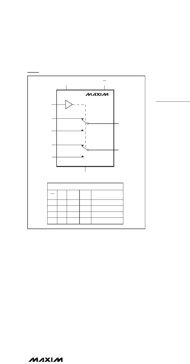
Functional Diagram/Truth Table