Technical Note
5/11
BU90LV047A
www.rohm.com
2011.12 - Rev.
© 2011 ROHM Co., Ltd. All rights reserved.
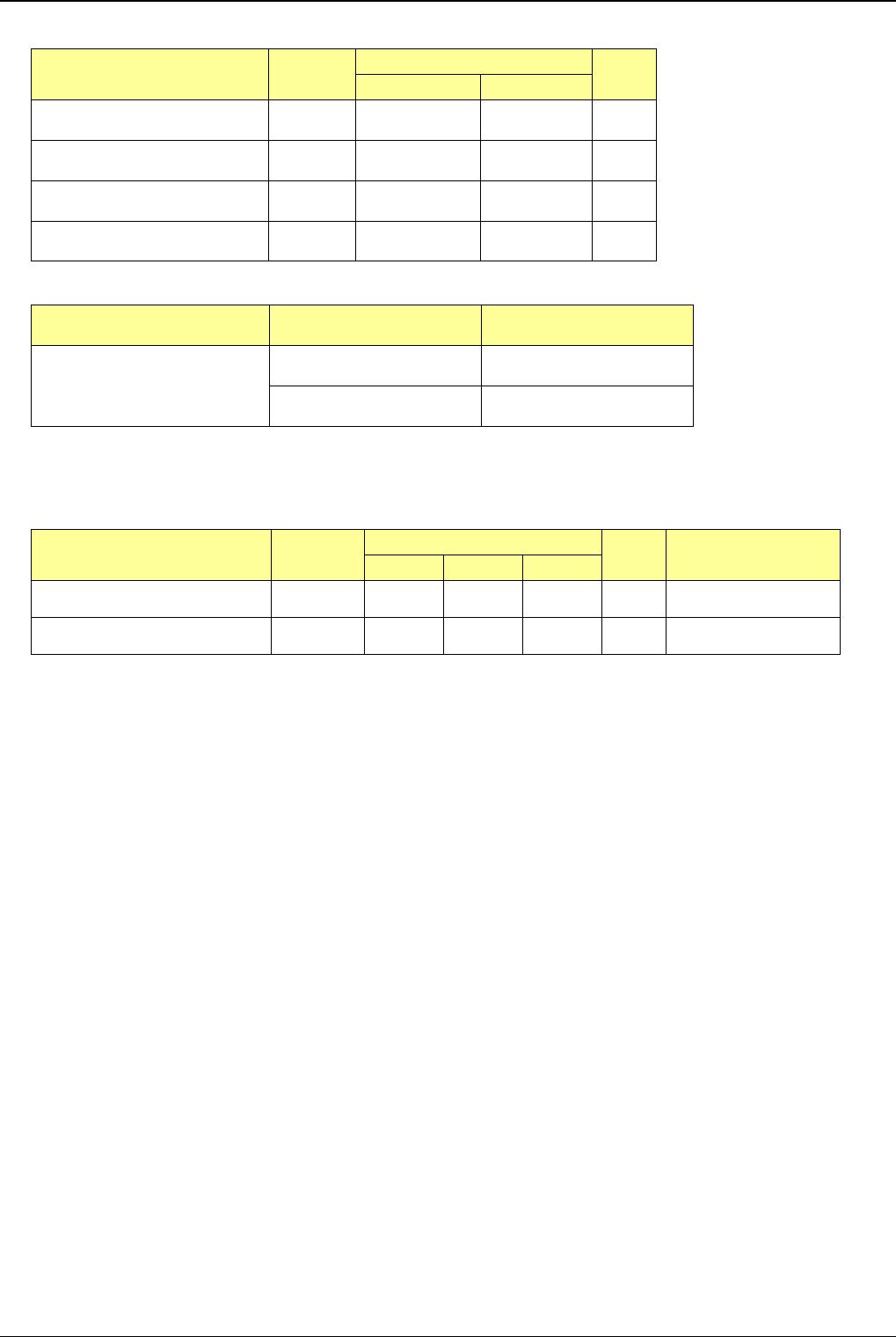
●Pin Description
Table 1 : Pin Description
Pin Name Pin No. Type Descriptions
DIN 2, 3, 6, 7
LVCMOS In
Driver input pin, LVCMOS compatible
DOUT+ 10, 11, 14, 15
LVDS Out
Non-inverting driver output pin,
LVDS levels
DOUT- 9, 12, 13, 16
LVDS Out
Inverting driver output pin, LVDS levels
SL 8
LVCMOS In
Swing Level select pin : When SL is high, the driver is reduce swing
level (200mV). When SL is low or open, the driver is normal swing
level (350mV).
EN 1
LVCMOS In
Driver enable pin: When EN is low or open, the driver is disabled.
When EN is high, the driver is enabled.
VCC 4
Power
Power supply pin, 3.3V±0.3V
GND 5
GND
Ground pin
●Function Description
INPUT OUTPUTS
Swing Level
EN SL DIN DOUT+ DOUT-
H L or Open
L L H
350mV
H H L
H H
L L H
200mV
H H L
All other combinations of
EN, SL inputs
X Z Z