NCL30288
www.onsemi.com
4
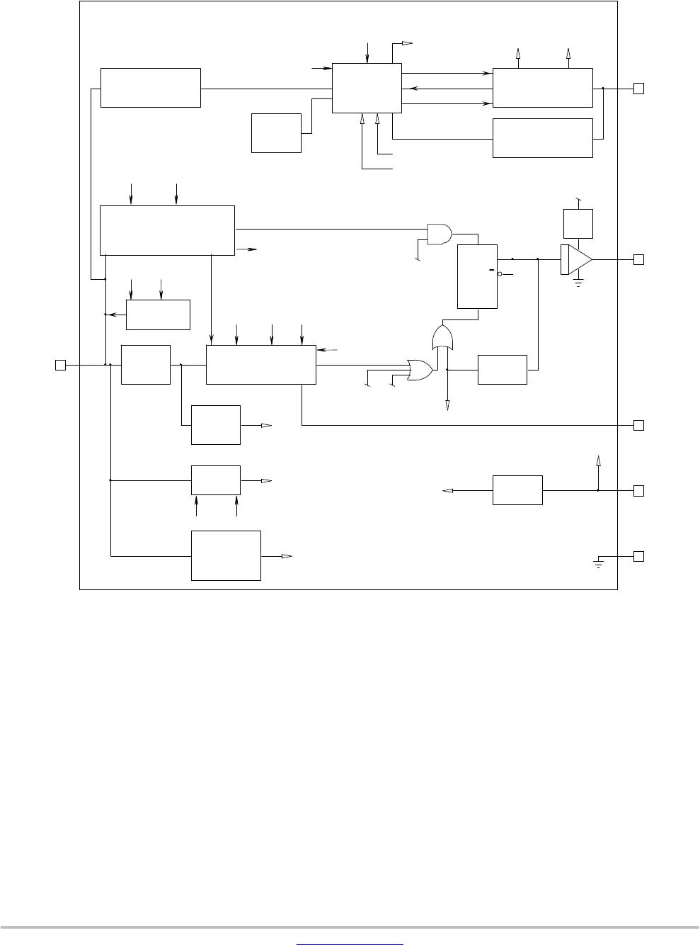
INTERNAL CIRCUIT ARCHITECTURE
Figure 3. Internal Circuit Architecture
ZCD
Over Voltage
Protection
Zero Crossing Detection Logic
(ZCD Blanking, Time−Out, ...)
CS/ZCD
Power Factor and
Constant−Current
Control
Leading
Edge
Blanking
Winding and
Output Diode
Short Circuit
Protection
Max. Peak
Current
Limit
Ipkmax
WOD_SCP
DRV
VCC Management
VCC
DRV
VCC Over Voltage
Protection
VCC
Internal
Thermal
Shutdown
Fault
Management
Clamp
Circuit
VS
Brown−Out
BO_NOK
S
R
Q
Q
CS_reset
STOP
UVLO
OFF
Latch
STOP
WOD_SCP
BO_NOK
GND
STOP
Aux. Winding Short Circuit Prot.
Aux_SCP
Aux_SCP
VCC_max
V
Line
feed−forward
VS
V
VS
Ipkmax
V
REF
V
DD
Enable
CS Short
Protection
CS_ok
CS_ok
FF_mode
Maximum
on time
UVLO
on,max
t
on,max
t
V
VS
COMP
V
REF
TF
V
DRV
NCL30288
www.onsemi.com
5
Table 2. MAXIMUM RATINGS TABLE
Symbol Rating Value Units
V
CC(MAX)
I
CC(MAX)
Maximum Power Supply voltage, V
CC
pin, continuous voltage
Maximum current for V
CC
pin
−0.3 to 30
Internally limited
V
mA
V
DRV(MAX)
I
DRV(MAX)
Maximum driver pin voltage, DRV pin, continuous voltage
Maximum current for DRV pin
−0.3, V
DRV
(Note 1)
−300, +500
V
mA
V
MAX
I
MAX
Maximum voltage on low power pins (except DRV and V
CC
pins)
Current range for low power pins (except DRV and V
CC
pins)
−0.3, 5.5 (Notes 2 and 5)
−2, +5
V
mA
R
θ
J−A
Thermal Resistance Junction−to−Air 360 °C/W
T
J(MAX)
Maximum Junction Temperature 150 °C
Operating Temperature Range −40 to +125 °C
Storage Temperature Range −60 to +150 °C
ESD Capability, Human Body Model (HBM) (Note 3) 3.5 kV
ESD Capability, Machine Model (MM) (Note 3) 250 V
Stresses exceeding those listed in the Maximum Ratings table may damage the device. If any of these limits are exceeded, device functionality
should not be assumed, damage may occur and reliability may be affected.
1. V
DRV
is the DRV clamp voltage V
DRV(high)
when V
CC
is higher than V
DRV(high)
. V
DRV
is V
CC
otherwise.
2. This level is low enough to guarantee not to exceed the internal ESD diode and 5.5 V ZENER diode. More positive and negative voltages
can be applied if the pin current stays within the −2 mA / 5 mA range.
3. This device contains ESD protection and exceeds the following tests: Human Body Model 3500 V per JEDEC Standard JESD22−A114E,
Machine Model Method 250 V per JEDEC Standard JESD22−A115B.
4. This device contains latch−up protection and exceeds 100 mA per JEDEC Standard JESD78.
5. Recommended maximum V
S
voltage for optimal operation is 4 V.
NCL30288
www.onsemi.com
6
Table 3. ELECTRICAL CHARACTERISTICS
(Unless otherwise noted: For typical values T
J
= 25°C, V
CC
= 12 V, V
CS/ZCD
= 0 V
For min/max values T
J
= −40°C to +125°C, Max T
J
= 150°C, V
CC
= 12 V)
Description
Test Condition Symbol Min Typ Max Unit
Startup and Supply Circuits
Supply Voltage
Startup Threshold
Minimum Operating Voltage
Hysteresis V
CC(on)
– V
CC(off)
Internal logic reset
V
CC
increasing
V
CC
decreasing
V
CC
decreasing
V
CC
decreasing
V
CC(on)
V
CC(off)
V
CC(HYS)
V
CC(reset)
16.0
8.2
8.0
4.0
18.0
8.8
4.8
20.0
9.4
6.0
V
Threshold for V
CC
Over Voltage Protection V
CC(OVP)
25.5 26.8 28.5 V
V
CC(off)
noise filter
V
CC(reset)
noise filter
t
VCC(off)
t
VCC(reset)
5
20
ms
Startup current V
CC
=15.9 V I
CC(start)
13 30
mA
Startup current in fault mode I
CC(sFault)
58 75
mA
Supply Current
Device Disabled / Fault
Device Enabled / No output load on pin 5
Device Switching
V
CC
> V
CC(off)
F
sw
= 65 kHz
C
DRV
= 470 pF, F
sw
= 65 kHz
I
CC1
I
CC2
I
CC3
1.15
1.34
2.0
2.5
1.55
3.5
4.0
mA
Current Sense
Maximum Internal current limit
V
ILIM
0.94 0.99 1.04 V
Leading Edge Blanking Duration for Current
Sensing
t
LEB
220 275 340 ns
Propagation delay from current detection to gate
off−state
t
ILIM
100 150 ns
Maximum on−time t
on(MAX)
26 36 46
ms
Threshold for immediate fault protection activation V
CS(stop)
1.35 1.50 1.65 V
Leading Edge Blanking Duration for V
CS(stop)
(Note 1)
t
BCS
175 ns
Current source for CS to GND short detection I
CS(short)
420 520 620
mA
Current sense threshold for CS to GND short
detection
V
CS
rising V
CS(low)
30 90 150 mV
Gate Drive
Drive Resistance
DRV Sink
DRV Source
R
SNK
R
SRC
13
30
W
Drive current capability
DRV Sink (Note GBD)
DRV Source (Note GBD)
I
SNK
I
SRC
500
300
mA
Rise Time (10 % to 90 %) C
DRV
= 470 pF t
r
40 ns
Fall Time (90 % to 10 %) C
DRV
= 470 pF t
f
30 ns
DRV Low Voltage V
CC
= V
CC(off)
+0.2 V
C
DRV
= 470 pF, R
DRV
=33 kW
V
DRV(low)
8 V
DRV High Voltage V
CC
= V
CC(MAX)
C
DRV
= 470 pF, R
DRV
=33 kW
V
DRV(high)
10 12 14 V
Zero Voltage Detection Circuit
Upper ZCD threshold voltage
V
ZCD
rising V
ZCD(rising)
90 150 mV
Lower ZCD threshold voltage V
ZCD
falling V
ZCD(falling)
35 55 mV
ZCD hysteresis V
ZCD(HYS)
15 mV

NCL30288BSNT1G

Mfr. #:
Manufacturer:
ON Semiconductor
Description:
LED Lighting Drivers HIGH PF PWM PRIMARY SIDE
Lifecycle:
New from this manufacturer.
Delivery:
DHL FedEx Ups TNT EMS
Payment:
T/T Paypal Visa MoneyGram Western Union

Products related to this Datasheet