DG9234EDQ-T1-GE3

DG9232E, DG9233E, DG9234E
www.vishay.com
Vishay Siliconix
S16-1451-Rev. A, 25-Jul-16
1
Document Number: 75165
For technical questions, contact: analogswitchtechsupport@vishay.com
THIS DOCUMENT IS SUBJECT TO CHANGE WITHOUT NOTICE. THE PRODUCTS DESCRIBED HEREIN AND THIS DOCUMENT
ARE SUBJECT TO SPECIFIC DISCLAIMERS, SET FORTH AT www.vishay.com/doc?91000
1 pC Charge Injection, 100 pA Leakage, +5 V / +3 V,
Dual SPST Analog Switches
DESCRIPTION
The DG9232E, DG9233E, and DG9234E are monolithic
CMOS switches designed for precision signal switching.
The 17 low voltage parts feature low charge injection,
leakage, parasitic capacitance, and fast switching.
The DG9232E, DG9233E, and DG9234E can switch both
analog and digital signals. Each switch conducts equally
well in both directions when on, and blocks up to the power
supply level when off.
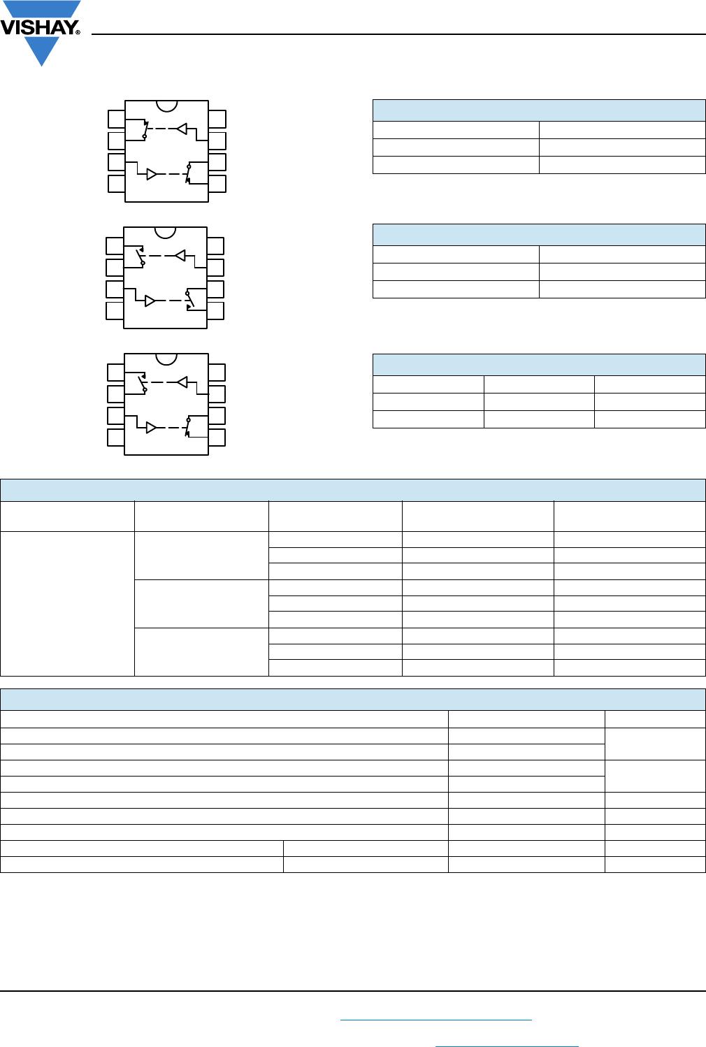
The DG9232E, DG9233E, and DG9234E contain two
independent single pole single throw (SPST) switches.
Switch-1 and switch-2 are normally closed for the DG9232E
and normally open for the DG9233E. For the DG9234E,
switch-1 is normally open and switch-2 is normally closed
with a break-before-make switching timing.
The DG9232E, DG9233E, and DG9234E offer 1 nW typical
power consumption and 8 kV ESD/HBM, 1 kV ESD/CDM
tolerance. They are the ideal switches for use in low voltage
instruments and healthcare devices, fitting the circuits of
low voltage ADC and DAC, sample and hold, analog front
end gain control, and signal path control. The DG9232E,
DG9233E, and DG9234E are available in 8-lead MSOP and
SOIC packages.
BENEFITS
Low charge injection and leakage
Low parasitic capacitance
Fast switching speed
High ESD tolerance
FEATURES
1 pC charge injection
Guaranteed 100 pA maximum switch on
leakage at 25 °C
3.8 pF switch off and 7.8 pF switch on
capacitances
+2.7 V to +5 V single supply operation
Low on-resistance - R
DS(on)
: 17 / typ. at 5 V
•t
ON
: 32 ns, t
OFF
: 10 ns switching time
Typical power consumption: 1 nW
Over voltage tolerant TTL / CMOS compatible
ESD (HBM): 8000 V, ESD (CDM): 1000 V
Latch-up current: > 300 mA (JESD78)
Available in MSOP-8 and SOIC-8
Material categorization: for definitions of compliance
please see www.vishay.com/doc?99912
Note
*
This datasheet provides information about parts that are
RoHS-compliant and / or parts that are non-RoHS-compliant. For
example, parts with lead (Pb) terminations are not RoHS-compliant.
Please see the information / tables in this datasheet for details.
APPLICATIONS
Automatic test equipment
Process control and automation
Data acquisition systems
Meters and instruments
Medical and healthcare systems
Communication systems
Sample-and-hold systems
Relay replacements
Battery powered systems
Available
Available
DG9232E, DG9233E, DG9234E
www.vishay.com
Vishay Siliconix
S16-1451-Rev. A, 25-Jul-16
2
Document Number: 75165
For technical questions, contact: analogswitchtechsupport@vishay.com
THIS DOCUMENT IS SUBJECT TO CHANGE WITHOUT NOTICE. THE PRODUCTS DESCRIBED HEREIN AND THIS DOCUMENT
ARE SUBJECT TO SPECIFIC DISCLAIMERS, SET FORTH AT www.vishay.com/doc?91000
FUNCTIONAL BLOCK DIAGRAM AND PIN CONFIGURATION
Logic “0” 0.8 V
Logic “1” 2.4 V
Logic “0” 0.8 V
Logic “1” 2.4 V
Logic “0” 0.8 V
Logic “1” 2.4 V
Notes
a. Signals on NC, NO, or COM or IN exceeding V+ will be clamped by internal diodes. Limit forward diode current to maximum current ratings.
b. All leads welded or soldered to PC board.
c. Derate 6.5 mW/°C above 70 °C.
Stresses beyond those listed under “Absolute Maximum Ratings” may cause permanent damage to the device. These are stress ratings only, and functional operation
of the device at these or any other conditions beyond those indicated in the operational sections of the specifications is not implied. Exposure to absolute maximum
rating conditions for extended periods may affect device reliability.
NC
1
V+
COM
1
IN
1
IN
2
COM
2
GND
NC
2
1
2
3
4
8
7
6
5
Top view
NO
1
V+
COM
1
IN
1
IN
2
COM
2
GND
NO
2
1
2
3
4
8
7
6
5
Top view
V+
GND
1
2
3
4
8
7
6
5
Top view
NO
1
COM
1
IN
1
IN
2
COM
2
NC
2
TRUTH TABLE - DG9232E
LOGIC SWITCH
0 On
1Off
TRUTH TABLE - DG9233E
LOGIC SWITCH
0 Off
1On
TRUTH TABLE - DG9234E
LOGIC SWITCH-1 SWITCH-2
0 Off On
1OnOff
ORDERING INFORMATION
TEMPERATURE
RANGE
CONFIGURATION PACKAGE PART NUMBER
MINIMUM ORDER /
PACKAGE QUANTITY
-40 °C to +85 °C
lead (Pb)-free
DG9232E
8-pin MSOP DG9232EDQ-T1-GE3 Tape and reel 2500 units
8-pin SOIC DG9232EDY-T1-GE3 Tape and reel 2500 units
8-pin SOIC DG9232EDY-GE3 Tube 500 units
DG9233E
8-pin MSOP DG9233EDQ-T1-GE3 Tape and reel 2500 units
8-pin SOIC DG9233EDY-T1-GE3 Tape and reel 2500 units
8-pin SOIC DG9233EDY-GE3 Tube 500 units
DG9234E
8-pin MSOP DG9234EDQ-T1-GE3 Tape and reel 2500 units
8-pin SOIC DG9234EDY-T1-GE3 Tape and reel 2500 units
8-pin SOIC DG9234EDY-GE3 Tube 500 units
ABSOLUTE MAXIMUM RATINGS
PARAMETER LIMIT UNIT
Reference V+ to GND -0.3 to +6
V
IN, COM, NC, NO
a
-0.3 to (V+ + 0.3)
Continuous current (any terminal) ± 20
mA
Peak current (pulsed at 1 ms, 10 % duty cycle) ± 40
ESD (HBM) (MIL-STD-883, method 3015) > 8000 V
ESD (CDM) (ANSI / ESDA / JEDEC
®
JS-002) > 1000 V
Latch up current, per JESD78 300 mA
Storage temperature D suffix -65 to +125 °C
Power dissipation (packages)
b
8-pin narrow body SOIC
c
400 mW
DG9232E, DG9233E, DG9234E
www.vishay.com
Vishay Siliconix
S16-1451-Rev. A, 25-Jul-16
3
Document Number: 75165
For technical questions, contact: analogswitchtechsupport@vishay.com
THIS DOCUMENT IS SUBJECT TO CHANGE WITHOUT NOTICE. THE PRODUCTS DESCRIBED HEREIN AND THIS DOCUMENT
ARE SUBJECT TO SPECIFIC DISCLAIMERS, SET FORTH AT www.vishay.com/doc?91000
Notes
a. Room = 25 °C, full = as determined by the operating suffix.
b. Typical values are for design aid only, not guaranteed nor subject to production testing.
c. The algebraic convention whereby the most negative value is a minimum and the most positive a maximum, is used in this datasheet.
d. Guarantee by design, nor subjected to production test.
e. V
IN
= input voltage to perform proper function.
f. Difference of min. and max. values.
g. Guaranteed by 5 V leakage tests, not production tested.
SPECIFICATIONS (V+ = 3 V)
PARAMETER SYMBOL
TEST CONDITIONS
OTHERWISE UNLESS SPECIFIED
V+ = 3 V, ± 10 %, V
IN
= 0.8 V or 2.4 V
e
TEMP.
a
D SUFFIX
-40 °C to +85 °C
UNIT
MIN.
c
TYP.
b
MAX.
c
Analog Switch
Analog signal range
d
V
ANALOG
Full 0 - 3 V
Drain-source on-resistance R
DS(on)
V
NO
or V
NC
= 1.5 V, V+ = 2.7 V
I
COM
= 5 mA
Room - 35 50
Full - 35 65
R
DS(on)
match
d
R
DS(on)
V
NO
or V
NC
= 1.5 V Room - 0.4 2
R
DS(on)
flatness
d
R
DS(on)
flatness
V
NO
or V
NC
= 1 V and 2 V Room - 4 8
NO or NC off leakage current
g
I
NO/NC(off)
V
NO
or V
NC
= 1 V/2 V, V
COM
= 2 V/1 V
Room -100 5 100
pA
Full -5000 5 5000
COM off leakage current
g
I
COM(off)
V
COM
= 1 V/2 V, V
NO
or V
NC
= 2 V/1 V
Room -100 5 100
Full -5000 5 5000
Channel-on leakage current
g
I
COM(on)
V
COM
= V
NO
or V
NC
= 1 V/2 V
Room -200 5 200
Full -10 000 5 10 000
Digital Control
Input current I
INL
or I
INH
Full - 0.001 - μA
Dynamic Characteristics
Turn-on time t
ON
V
NO
or V
NC
= 1.5 V
Room - 43 120
ns
Full - - 200
Turn-off time t
OFF
Room - 16 50
Full - - 120
Charge injection
d
Q
INJ
C
L
= 1 nF, V
GEN
= 0 V, R
GEN
= 0 Room - -0.28 - pC
Off-isolation OIRR
R
L
= 50 , C
L
= 5 pF, f = 1 MHz
Room - -80 -
dB
Crosstalk X
TALK
Room - -108 -
NC and NO capacitance C
S(off)
f = 1 MHz
Room - 4 -
pFChannel-on capacitance C
COM(on)
Room - 8 -
COM-off capacitance C
COM(off)
Room - 4 -
Power Supply
Positive supply range V+ 2.7 - 5.5 V
Power supply current I+ V+ = 3.3 V, V
IN
= 0 V or 3.3 V 0.0003 - 1 μA

DG9234EDQ-T1-GE3

Mfr. #:
Manufacturer:
Vishay / Siliconix
Description:
Analog Switch ICs Dual SPST Switch 1pC charge injection
Lifecycle:
New from this manufacturer.
Delivery:
DHL FedEx Ups TNT EMS
Payment:
T/T Paypal Visa MoneyGram Western Union