LTC1690CS8#PBF

7
LTC1690
SWITCHI G TI E WAVEFOR S
UWW
–V
O
D
3V
0V
t
PLH
V
O
= V(A) – V(B)
V
O
Z
Y
t
SKEW
t
SKEW
t
r
f = 1MHz, t
r
10ns, t
f
10ns
1.5V
90%
10%
50%
t
PHL
t
f
1.5V
90%
10%
50%
V
O
1/2 V
O
1690 F04
Figure 4. Driver Propagation Delays
f = 1MHz, t
r
10ns, t
f
10ns
NOTE: t
SKD
= |t
PHL
– t
PLH
|
INPUT
OUTPUT
A – B
R
V
OD2
–V
OD2
5V
V
OL
t
PHL
0V
1.5V
t
PLH
0V
1.5V
1690 F05
Figure 5. Receiver Propagation Delays
FUNCTION TABLES
UU
Driver
DZY
101
010
Receiver
A – B R
0.01V 1
0.20V 0
Inputs Open 1
Inputs Shorted 1
Note: Table valid with or without termination resistors.
1690 F01
Y
Z
R
R
V
OD2
V
OC
1690 F02
Y
Z
60
375
V
OD3
V
TST
–7V TO 12V
375
1690 F03
D
Y
Z
R
DIFF
A
B
15pF
C
L1
C
L2
R
+
+
+
Figure 1. Driver
DC Test Load #1
Figure 2. Driver
DC Test Load #2
Figure 3. Driver/Receiver
Timing Test Load
TEST CIRCUITS
PIN FUNCTIONS
UUU
V
CC
(Pin 1): Positive Supply. 4.75V < V
CC
< 5.25V.
R (Pin 2): Receiver Output. R is high if (A – B) 10mV
and low if (A – B) 200mV.
D (Pin 3): Driver Input. If D is high, Y is taken high and Z
is taken low. If D is low, Y is taken low and Z is taken high.
GND (Pin 4): Ground.
Y (Pin 5): Driver Output.
Z (Pin 6): Driver Output.
B (Pin 7): Receiver Input.
A (Pin 8): Receiver Input.
8
LTC1690
3
1
5
6
D
120
2
1
8
7
RDRIVER
LTC1690
5V
LTC1690
RECEIVER
120
SHIELD
2
4
7
8
R
3
4
6
5
DRECEIVER DRIVER
1690 F06
SHIELD
0.01µF
5V
0.01µF
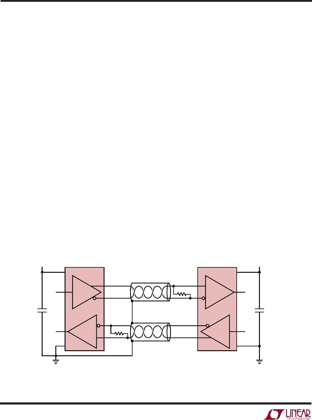
Figure 6. Typical Application
APPLICATIONS INFORMATION
WUU
U
A typical application is shown in Figure 6. Two twisted pair
wires connect two driver/receiver pairs for full duplex data
transmission. Note that the driver and receiver outputs are
always enabled. If the outputs must be disabled, use the
LTC491. There are no restrictions on where the chips are
connected, and it isn’t necessary to have the chips con-
nected to the ends of the wire. However, the wires must be
terminated at the ends with a resistor equal to their
characteristic impedance, typically 120. Because only
one driver can be connected on the bus, the cable need
only be terminated at the receiving end. The optional
shields around the twisted pair are connected to GND at
one end and help reduce unwanted noise.
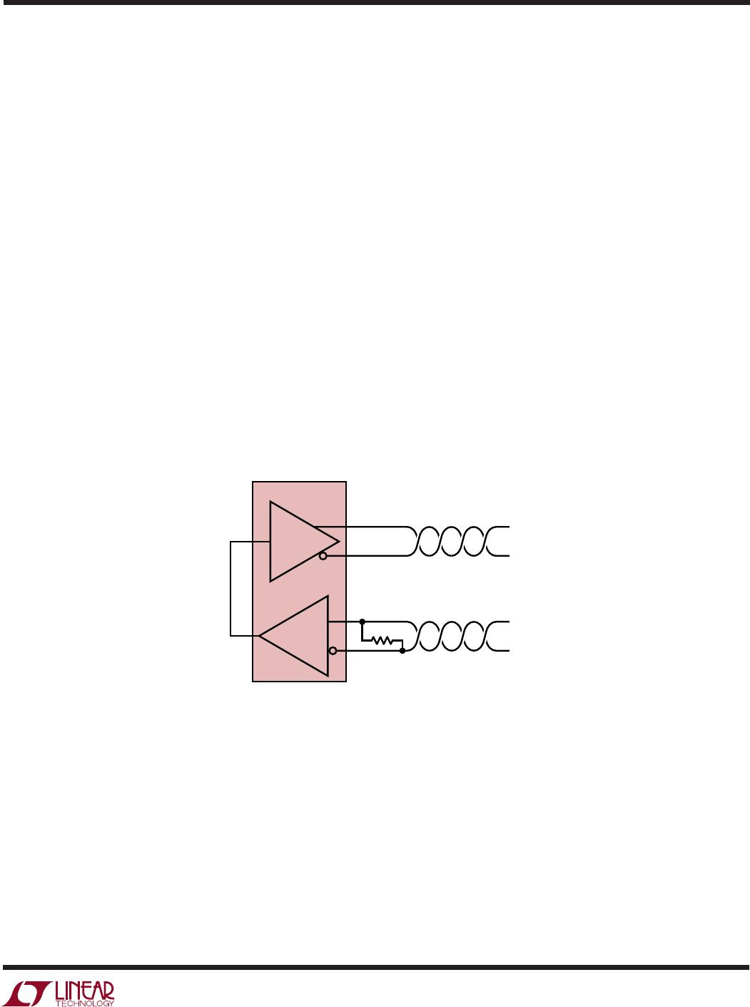
The LTC1690 can be used as a line repeater as shown in
Figure 7. If the cable is longer that 4000 feet, the LTC1690
is inserted in the middle of the cable with the receiver
output connected back to the driver input.
Receiver Fail-Safe
Some encoding schemes require that the output of the
receiver maintains a known state (usually a logic 1) when
data transmission ends and all drivers on the line are
forced into three-state. The receiver of the LTC1690 has a
fail-safe feature which guarantees the output to be in a
logic 1 state when the receiver inputs are left floating or
shorted together. This is achieved without external com-
ponents by designing the trip-point of the LTC1690 to be
within –200mV to –10mV. If the receiver output must be
a logic 0 instead of a logic 1, external components are
required.
The LTC1690 fail-safe receiver is designed to reject fast
7V to 12V common mode steps at its inputs. The slew
rate that the receiver will reject is typically 400V/µs, but
7V to 12V steps in 10ns can be tolerated if the frequency
of the common mode step is moderate (<600kHz).
Driver-Receiver Crosstalk
The driver outputs generate fast rise and fall times. If the
LTC1690 receiver inputs are not terminated and floating,
switching noise from the LTC1690 driver can couple into
the receiver inputs and cause the receiver output to glitch.
This can be prevented by ensuring that the receiver inputs
are terminated with a 100 or 120 resistor, depending
on the type of cable used. A cable capacitance that is
greater than 10pF (1ft of cable) also prevents glitches if
no termination is present. The receiver inputs should not
be driven typically above 8MHz to prevent glitches.
9
LTC1690
APPLICATIONS INFORMATION
WUU
U
Fault Protection
When shorted to –7V or 10V at room temperature, the
short-circuit current in the driver outputs is limited by
internal resistance or protection circuitry to 250mA maxi-
mum. Over the industrial temperature range, the absolute
maximum positive voltage at any driver output should be
limited to 10V to avoid damage to the driver outputs. At
higher ambient temperatures, the rise in die temperature
due to the short-circuit current may trip the thermal
shutdown circuit.
The receiver inputs can withstand the entire –7V to 12V
RS485 common mode range without damage.
The LTC1690 includes a thermal shutdown circuit that
protects the part against prolonged shorts at the driver
outputs. If a driver output is shorted to another output or
to V
CC
, the current will be limited to a maximum of 250mA.
If the die temperature rises above 150°C, the thermal
shutdown circuit three-states the driver outputs to open
the current path. When the die cools down to about 130°C,
the driver outputs are taken out of three-state. If the short
persists, the part will heat again and the cycle will repeat.
This thermal oscillation occurs at about 10Hz and protects
the part from excessive power dissipation. The average
fault current drops as the driver cycles between active and
three-state. When the short is removed, the part will return
to normal operation.
If the outputs of two or more LTC1690 drivers are shorted
directly, the driver outputs cannot supply enough current
to activate the thermal shutdown. Thus, the thermal shut-
down circuit will not prevent contention faults when two
drivers are active on the bus at the same time.
3
5
6
D DRIVER
LTC1690
120
2
8
7
R
RECEIVER
DATA
OUT
DATA
IN
1690 F07
Figure 7. Line Repeater

LTC1690CS8#PBF

Mfr. #:
Manufacturer:
Analog Devices Inc.
Description:
RS-422/RS-485 Interface IC Diff Drvr & Rcv Pair w/ Fail-Safe Rcv O
Lifecycle:
New from this manufacturer.
Delivery:
DHL FedEx Ups TNT EMS
Payment:
T/T Paypal Visa MoneyGram Western Union