REV. B
CMP401/CMP402
–4–
CAUTION
ESD (electrostatic discharge) sensitive device. Electrostatic charges as high as 4000 V readily
accumulate on the human body and test equipment and can discharge without detection. Although
the CMP401/CMP402 features proprietary ESD protection circuitry, permanent damage may
occur on devices subjected to high-energy electrostatic discharges. Therefore, proper ESD precautions
are recommended to avoid performance degradation or loss of functionality.
WARNING!
ESD SENSITIVE DEVICE
ABSOLUTE MAXIMUM RATINGS
1
Total Analog Supply Voltage . . . . . . . . . . . . . . . . . . . . . . 16 V
Digital Supply Voltage . . . . . . . . . . . . . . . . . . . . . . . . . . . . 7 V
Analog Positive Supply—Digital Positive Supply . . . . –200 mV
Input Voltage
2
. . . . . . . . . . . . . . . . . . . . . . . . . . . . . . . . . ± 7 V
Differential Input Voltage . . . . . . . . . . . . . . . . . . . . . . . . ± 9 V
Output Short-Circuit Duration to GND . . . . . . . . . Indefinite
Storage Temperature Range
S, RU Package . . . . . . . . . . . . . . . . . . . . . –65°C to +150°C
Operating Temperature Range
CMP401G, CMP402G . . . . . . . . . . . . . . –40°C to +125°C
Junction Temperature Range
S, RU Package . . . . . . . . . . . . . . . . . . . . . –65°C to +150°C
Lead Temperature Range (Soldering 60 sec) . . . . . . . . . 300°C
JA
3
JC
Units
113 37 °C/W
Package Type
16-Lead SOIC (S)
16-Lead TSSOP (RU) 180 37 °C/W
NOTES
1
Absolute Maximum Ratings apply to packaged parts, unless otherwise noted.
2
The analog input voltage is equal to ± 7 V or the analog supply voltage, whichever
is less.
3
JA
is specified for the worst-case conditions, i.e.,
JA
is specified for device soldered
in circuit board for SOIC and TSSOP packages.
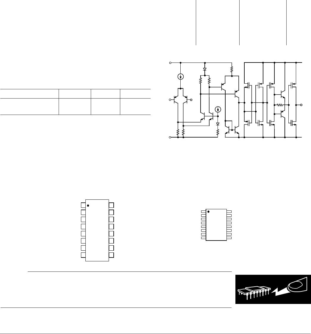
PIN CONFIGURATIONS
16-Lead Narrow-SOIC
(S-Suffix)
14
13
12
11
16
15
10
9
8
1
2
3
4
7
6
5
OUT B
OUT A
V+ DIG
V+ ANA
–IN A
+IN A
–IN B
+IN B
V– ANA
DIG GND
OUT D
OUT C
–IN C
+IN D
–IN D
+IN C
TOP VIEW
(Not to Scale)
CMP401/
402
16-Lead
TSSOP
(RU-Suffix)
OUT B
OUT A
V+ DIG
V+ ANA
–IN A
+IN A
–IN B
+IN B
V– ANA
DIG GND
OUT D
OUT C
–IN C
+IN D
–IN D
+IN C
116
8
9
TOP VIEW
(Not to Scale)
CMP401/
402
+IN
–IN
V+ ANA
V– ANA
V+ DIG
OUT
DIG GND
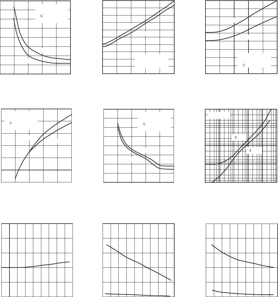
Figure 1. Simplified Schematic
Revision History
Location
Page
Data Sheet changed from REV. 0 to REV. A.
Changed SO-16 to 16-Lead SOIC . . . . . . . . . . . . .Throughout
Edits to GENERAL DESCRIPTION . . . . . . . . . . . . . . . . . . .1
Moved Outline Dimensions . . . . . . . . . . . . . . . . . . . . . . . . . . . . . . 8
Edits to ABSOLUTLE MAXIMUM RATINGS . . . . . . . . . .4
Edits to PACKAGE TYPE. . . . . . . . . . . . . . . . . . . . . . . . . . . 4
Edits to ORDERING GUIDE . . . . . . . . . . . . . . . . . . . . . . . . 4
Deleted DICE CHARACTERISTICS . . . . . . . . . . . . . . . . . 4
Edits to CMP401/CMP402 PIN CONFIRGURATIONS. . 4
Data Sheet changed from REV. A to REV. B.
Updated Outline Dimensions . . . . . . . . . . . . . . . . . . . . . . . . . . . . 8
Changes to Ordering Guide . . . . . . . . . .. . . . . . . . . . . . . . . . 8
Moved Revision History . . . . . . . . . . . . . . . . . . . . . . . . . . . . . . . . . 4
Location
Page