8
Notes:
General Note: Typical values represent the mean value of all char-
acterization units at the nominal operating conditions. Typical drift
specications are determined by calculating the rate of change of the
specied parameter versus the drift parameter (at nominal operating
conditions) for each characterization unit, and then averaging the indi-
vidual unit rates. The corresponding drift gures are normalized to the
nominal operating conditions and show how much drift occurs as the
particular drift parameter is varied from its nominal value, with all other
parameters held at their nominal operating values. Note that the typical
drift specications in the tables may dier from the slopes of the mean
curves shown in the corresponding gures.
1. It is recommended to operate with V
IN–
= 0 V (tied to GND1). Limiting
V
IN+
to 100 mV will improve DC nonlinearity and nonlinearity drift.
If V
IN–
is brought above V
DD1
– 2 V, an internal test mode may be
activated. This test mode is for LED coupling test and is not intended
for customer use.
2. This is the Absolute Value of Input Oset Change vs. Temperature.
3. Gain is dened as the slope of the best-t line of dierential output
voltage (V
OUT+
–V
OUT–
) vs. dierential input voltage (V
IN+
–V
IN–
) over
the specied input range.
4. This is the Absolute Value of Gain Change vs. Temperature.
5. Nonlinearity is dened as half of the peak-to-peak output deviation
from the best-t gain line, expressed as a percentage of the full-scale
dierential output voltage.
6. NL
100
is the nonlinearity specied over an input voltage range of
±100 mV.
7. The input supply current decreases as the dierential input voltage
(V
IN+
–V
IN–
) decreases.
8. The maximum specied output supply current occurs when the
dierential input voltage (V
IN+
–V
IN–
) = –200 mV, the maximum
recommended operating input voltage. However, the output supply
current will continue to rise for dierential input voltages up to
approximately –300 mV, beyond which the output supply current
remains constant.
9. Because of the switched-capacitor nature of the input sigma-delta
converter, time-averaged values are shown.
10. When the dierential input signal exceeds approximately 308 mV,
the outputs will limit at the typical values shown.
11. Short circuit current is the amount of output current generated when
either output is shorted to V
DD2
or GND2.
12. CMRR is dened as the ratio of the dierential signal gain (signal
applied dierentially between pins 2 and 3) to the common-mode
gain (input pins tied together and the signal applied to both inputs
at the same time), expressed in dB.
13. Output noise comes from two primary sources: chopper noise and
sigma-delta quantization noise. Chopper noise results from chopper
stabilization of the output op-amps. It occurs at a specic frequency
(typically 400 kHz at room temperature), and is not attenuated by
the internal output lter. A lter circuit can be easily added to the
external post-amplier to reduce the total RMS output noise. The
internal output lter does eliminate most, but not all, of the sigma-
delta quantization noise. The magnitude of the output quantization
noise is very small at lower frequencies (below 10 kHz) and increases
with increasing frequency.
14. CMTI (Common Mode Transient Immunity or CMR, Common Mode
Rejection) is tested by applying an exponentially rising/falling voltage
step on pin 4 (GND1) with respect to pin 5 (GND2). The rise time of
the test waveform is set to approximately 50 ns. The amplitude of the
step is adjusted until the dierential output (V
OUT+
–V
OUT–
) exhibits
more than a 200 mV deviation from the average output voltage for
more than 1μs. The ACPL-C78A/C780/C784 will continue to function
if more than 10 kV/μs common mode slopes are applied, as long as
the breakdown voltage limitations are observed.
15. Data sheet value is the dierential amplitude of the transient at the
output of the ACPL-C78A/C780/C784 when a 1 Vpk-pk, 1 MHz square
wave with 40 ns rise and fall times is applied to both V
DD1
and V
DD2
.
16. In accordance with UL 1577, each optocoupler is proof tested by
applying an insulation test voltage ≥6000 Vrms for 1 second (leakage
detection current limit, I
I-O
≤ 5 μA). This test is performed before the
100% production test for partial discharge (method b) shown in IEC/
EN/DIN EN 60747-5-5 Insulation Characteristic Table.
17. The Input-Output Momentary Withstand Voltage is a dielectric
voltage rating that should not be interpreted as an input-output
continuous voltage rating. For the continuous voltage rating, refer
to the IEC/EN/DIN EN 60747-5-5 insulation characteristics table and
your equipment level safety specication.
18. This is a two-terminal measurement: pins 1–4 are shorted together
and pins 5–8 are shorted together.
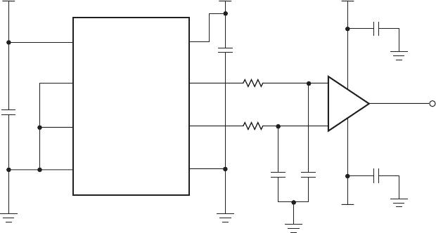
Figure 1. Input Oset Voltage Test Circuit.
0.1 µF
V
DD2
V
OUT
8
7
6
1
3
ACPL-C78A
ACPL-C780
ACPL-C784
5
2
4
0.1 µF
10 K
10 K
V
DD1
+15 V
0.1 µF
0.1 µF
-15 V
+
–
AD624CD
GAIN = 100
0.47
µF
0.47
µF