12
Application Information
Power Supplies and Bypassing
The recommended supply connections are shown in
Figure 17. A oating power supply (which in many ap-
plications could be the same supply that is used to drive
the high-side power transistor) is regulated to 5 V using
a simple zener diode (D1); the value of resistor R4 should
be chosen to supply sucient current from the existing
oating supply. The voltage from the current sensing
resistor (Rsense) is applied to the input of the ACPL-C78A/
C780/C784 through an RC anti-aliasing lter (R2 and C2).
Although the application circuit is relatively simple, a few
recommendations should be followed to ensure optimal
performance.
The power supply for the ACPL-C78A/C780/C784 is most
often obtained from the same supply used to power the
power transistor gate drive circuit. If a dedicated supply is
required, in many cases it is possible to add an additional
winding on an existing transformer. Otherwise, some sort of
simple isolated supply can be used, such as a line powered
transformer or a high-frequency DC-DC converter.
An inexpensive 78L05 three-terminal regulator can also be
used to reduce the oating supply voltage to 5 V. To help
attenuate high-frequency power supply noise or ripple, a
resistor or inductor can be used in series with the input of
the regulator to form a low-pass lter with the regulator’s
input bypass capacitor.
As shown in Figure 18, 0.1 μF bypass capacitors (C1, C2)
should be located as close as possible to the pins of the
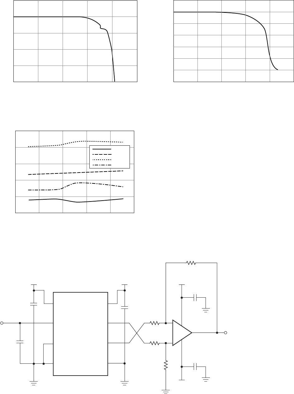
Figure 16. CMTI Test Circuits.
0.1 µF
V
DD2
V
OUT
8
7
6
1
3
ACPL-C78A
ACPL-C780
ACPL-C784
5
2
4
2 K
2 K
78L05
+15 V
0.1 µF
0.1 µF
-15 V
–
+
MC34081
150
pF
IN OUT
0.1
µF
0.1
µF
9 V
PULSE GEN.
V
CM
+
–
10 K
10 K
150 pF
ACPL-C78A/C780/C784. The bypass capacitors are
required because of the high-speed digital nature of
the signals inside the ACPL-C78A/C780/C784. A 0.01 μF
bypass capacitor (C2) is also recommended at the input
due to the switched-capacitor nature of the input circuit.
The input bypass capacitor also forms part of the anti-
aliasing lter, which is recommended to prevent high-
frequency noise from aliasing down to lower frequencies
and interfering with the input signal. The input lter also
performs an important reliability function – it reduces
transient spikes from ESD events owing through the
current sensing resistor.
PC Board Layout
The design of the printed circuit board (PCB) should follow
good layout practices, such as keeping bypass capacitors
close to the supply pins, keeping output signals away from
input signals, the use of ground and power planes, etc. In
addition, the layout of the PCB can also aect the isolation
transient immunity (CMTI) of the ACPL-C78A/C780/C784,
due primarily to stray capacitive coupling between the
input and the output circuits. To obtain optimal CMTI
performance, the layout of the PC board should minimize
any stray coupling by maintaining the maximum possible
distance between the input and output sides of the circuit
and ensuring that any ground or power plane on the PC
board does not pass directly below or extend much wider
than the body of the ACPL-C78A/C780/C784.