RJK0355DSP
REJ03G1650-0301 Rev.3.01 Apr 24, 2008
Page 2 of 6
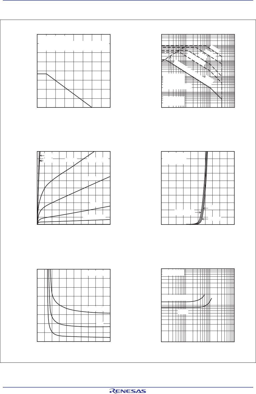
Electrical Characteristics
(Ta = 25°C)
Item Symbol Min Typ Max Unit Test Conditions
Drain to source breakdown voltage V
(BR)DSS
30 — — V I
D
= 10 mA, V
GS
= 0
Gate to source leak current I
GSS
— — ± 0.1 µA V
GS
= ±20 V, V
DS
= 0
Zero gate voltage drain current I
DSS
— — 1 µA V
DS
= 30 V, V
GS
= 0
Gate to source cutoff voltage V
GS(off)
1.2 — 2.5 V V
DS
= 10 V,
I
D
= 1 mA
R
DS(on)
— 8.5 11.1 mΩ I
D
= 6 A, V
GS
= 10 V
Note4
Static drain to source on state
resistance
R
DS(on)
— 12.0 16.8 mΩ I
D
= 6 A, V
GS
= 4.5 V
Note4
Forward transfer admittance |y
fs
| — 35 — S I
D
= 6 A, V
DS
= 10 V
Note4
Input capacitance Ciss — 860 — pF
Output capacitance Coss — 165 — pF
Reverse transfer capacitance Crss — 53 — pF
V
DS
= 10 V
V
GS
= 0
f = 1 MHz
Gate Resistance Rg — 4.2 — Ω
Total gate charge Qg — 6.0 — nC
Gate to source charge Qgs — 2.3 — nC
Gate to drain charge Qgd — 1.4 — nC
V
DD
= 10 V
V
GS
= 4.5 V
I
D
= 6 A
Turn-on delay time t
d(on)
— 6.9 — ns
Rise time t
r
— 3.5 — ns
Turn-off delay time t
d(off)
— 40.2 — ns
Fall time t
f
— 4.8 — ns
V
GS
= 10 V, I
D
= 6 A
V
DD
≅ 10 V
R
L
= 1.67 Ω
Rg = 4.7 Ω
Body–drain diode forward voltage V
DF
— 0.82 1.07 V I
F
= 12 A, V
GS
= 0
Note3
Body–drain diode reverse recovery
time
t
rr
— 20 — ns
I
F
= 12 A, V
GS
= 0
di
F
/ dt = 100 A/ µs
Notes: 4. Pulse test