Si824x
Preliminary Rev. 0.3 19
3.4. Power Supply Connections
Isolation requirements mandate individual supplies for VDDI, VDDA, and VDDB. The decoupling caps for these
supplies must be placed as close to the VDD and GND pins of the Si824x as possible. The optimum values for
these capacitors depend on load current and the distance between the chip and the regulator that powers it. Low
effective series resistance (ESR) capacitors, such as Tantalum, are recommended.
3.5. Power Dissipation Considerations
Proper system design must assure that the Si824x operates within safe thermal limits across the entire load range.
The Si824x total power dissipation is the sum of the power dissipated by bias supply current, internal switching
losses, and power delivered to the load. Equation 1 shows total Si824x power dissipation. In a non-overlapping
system, such as a high-side/low-side driver, n = 1.
Equation 1.
The maximum power dissipation allowable for the Si824x is a function of the package thermal resistance, ambient
temperature, and maximum allowable junction temperature, as shown in Equation 2:
Equation 2.
Substituting values for P
Dmax
T
jmax
, T
A
, and
ja
into Equation 2 results in a maximum allowable total power
dissipation of 1.19 W. Maximum allowable load is found by substituting this limit and the appropriate datasheet
values from Table 1 on page 5 into Equation 1 and simplifying. The result is Equation 3 (0.5 A driver) and
Equation 4 (4.0 A driver), both of which assume VDDI = 5 V and VDDA = VDDB = 18 V.
Equation 3.
Equation 4.
P
D
V
DDI
I
DDI
2V
DDO
I
QOUT
C
int
V
DDO
2
F+2n C
L
V
DDO
2
F++
where:
P
D
is the total Si824x device power dissipation (W)
I
DDI
is the input-side maximum bias current (3 mA)
I
QOUT
is the driver die maximum bias current (2.5 mA)
C
int
is the internal parasitic capacitance (75 pF for the 0.5 A driver and 370 pF for the 4.0 A driver)
V
DDI
is the input-side VDD supply voltage (4.5 to 5.5 V)
V
DDO
is the driver-side supply voltage (10 to 24 V)
F is the switching frequency (Hz)
n is the overlap constant (max value = 2)
=
P
Dmax
T
jmax
T
A
ja
---------------------------
where:
P
Dmax
= Maximum Si824x power dissipation (W)
T
jmax
= Si824x maximum junction temperature (150 °C)
T
A
= Ambient temperature (°C)
ja = Si824x junction-to-air thermal resistance (105 °C/W)
F = Si824x switching frequency (Hz)
C
L(MAX)
1.4 10
3
F
--------------------------
7.5 10
11
=
C
L(MAX)
1.4 10
3
F
--------------------------
3.7 10
10
=
Si824x
20 Preliminary Rev. 0.3
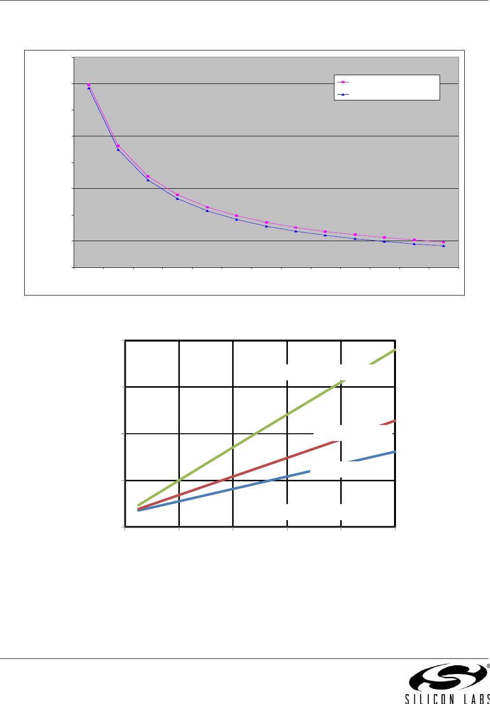
Equation 1 and Equation 2 are graphed in Figure 32 where the points along the load line represent the package
dissipation-limited value of CL for the corresponding switching frequency.
Figure 32. Max Load vs. Switching Frequency
Figure 33. Switching Frequency vs. Load Current
0
2,000
4,000
6,000
8,000
10,000
12,000
14,000
16,000
100
150
200
250
300
350
400
450
500
550
600
650
700
Frequency (Khz)
Max Load (pF)
0.5A Driver (pF)
4A Driver (pF)
T
a
= 25 °C
0
5
10
15
20
0 200 400 600 800 1000
VDDA Supply Current (mA)
Switching Frequency (kHz)
VDD=15V, 25°C
C
L
= 1000pF
C
L
= 500pF
C
L
= 200pF
Si824x
Preliminary Rev. 0.3 21
3.6. Layout Considerations
It is most important to minimize ringing in the drive path and noise on the Si824x VDD lines. Care must be taken to
minimize parasitic inductance in these paths by locating the Si824x as close to the device it is driving as possible.
In addition, the VDD supply and ground trace paths must be kept short. For this reason, the use of power and
ground planes is highly recommended. A split ground plane system having separate ground and VDD planes for
power devices and small signal components provides the best overall noise performance.
3.7. Undervoltage Lockout Operation
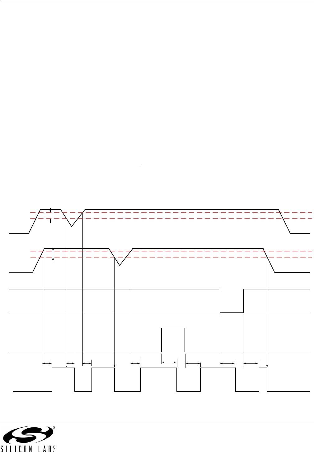
Device behavior during start-up, normal operation and shutdown is shown in Figure 34, where UVLO+ and UVLO-
are the positive-going and negative-going thresholds respectively. Note that outputs VOA and VOB default low
when input side power supply (VDDI) is not present.
3.7.1. Device Startup
Outputs VOA and VOB are held low during power-up until VDD is above the UVLO threshold for time period
tSTART. Following this, the outputs follow the states of inputs VIA and VIB.
3.7.2. Undervoltage Lockout
Undervoltage Lockout (UVLO) is provided to prevent erroneous operation during device startup and shutdown or
when VDD is below its specified operating circuits range. The input (control) side, Driver A and Driver B, each have
their own undervoltage lockout monitors.
The Si824x input side enters UVLO when VDDI <
VDDI
UV–
, and exits UVLO when VDDI > VDDI
UV+
. The driver
outputs, VOA and VOB, remain low when the input side of the Si824x is in UVLO and their respective VDD supply
(VDDA, VDDB) is within tolerance. Each driver output can enter or exit UVLO independently. For example, VOA
unconditionally enters UVLO when VDDA falls below VDDA
UV–
and exits UVLO when VDDA rises above
VDDA
UV+
.
Figure 34. Device Behavior during Normal Operation and Shutdown
PWM
VOA
DISABLE
VDDI
UVLO-
VDDA
tSTART tSTART tSTART
tSD tRESTART
tPHL tPLH
UVLO+
UVLO-
UVLO+
tSD
VDD
HYS
VDD
HYS

SI8244CB-D-IS1R

Mfr. #:
Manufacturer:
Silicon Labs
Description:
Gate Drivers 2.5kV 4A Class D Audio Driver, 10V UVLO PWM input
Lifecycle:
New from this manufacturer.
Delivery:
DHL FedEx Ups TNT EMS
Payment:
T/T Paypal Visa MoneyGram Western Union