© Semiconductor Components Industries, LLC, 2013
July, 2013 − Rev. 9
1 Publication Order Number:
MMDL914T1/D
MMDL914T1G,
SMMDL914T1G,
MMDL914T3G
High-Speed Switching
Diode
Features
• S Prefix for Automotive and Other Applications Requiring Unique
Site and Control Change Requirements; AEC−Q101 Qualified and
PPAP Capable
• These Devices are Pb−Free, Halogen Free/BFR Free and are RoHS
Compliant
MAXIMUM RATINGS
Rating Symbol Value Unit
Reverse Voltage V
R
100 V
Forward Current I
F
200 mA
Non−Repetitive Peak Forward Surge
Current 60 Hz
I
FSM(surge)
500 mA
Repetitive Peak Forward Current
(Note 2)
I
FRM
1.0 A
Non−Repetitive Peak Forward Current
(Square Wave, T
J
= 25°C prior to
surge)
t = 1 ms
t = 10 ms
t = 100 ms
t = 1 ms
t = 1 s
I
FSM
36.0
18.0
6.0
3.0
0.7
A
THERMAL CHARACTERISTICS
Characteristic Symbol Max Unit
Total Device Dissipation FR-5 Board
T
A
= 25°C (Note 1)
Derate above 25°C
P
D
200
1.57
mW
mW/°C
Thermal Resistance,
Junction−to−Ambient
R
q
JA
635
°C/W
Junction and Storage Temperature T
J
, T
stg
−55 to 150 °C
Stresses exceeding Maximum Ratings may damage the device. Maximum
Ratings are stress ratings only. Functional operation above the Recommended
Operating Conditions is not implied. Extended exposure to stresses above the
Recommended Operating Conditions may affect device reliability.
1. FR-4 Minimum Pad.
2. Square Wave, f = 40 kHz, PW = 200 ns
Test Duration = 60 s, T
J
= 25°C prior to surge.
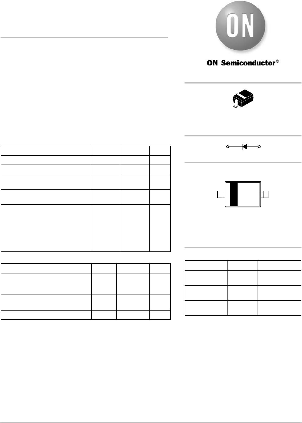
http://onsemi.com
SOD−323
CASE 477
STYLE 1
MARKING DIAGRAM
1
CATHODE
2
ANODE
Device Package Shipping
†
ORDERING INFORMATION
†For information on tape and reel specifications,
including part orientation and tape sizes, please
refer to our Tape and Reel Packaging Specifications
Brochure, BRD8011/D.
5D M G
G
MMDL914T1G SOD−323
(Pb−Free)
3,000 /
Tape & Reel
5D = Specific Device Code
M = Date Code
G = Pb−Free Package
(Note: Microdot may be in either location)
MMDL914T3G SOD−323
(Pb−Free)
10,000 /
Tape & Reel
SMMDL914T1G SOD−323
(Pb−Free)
3,000 /
Tape & Reel