DATA SHEET
IDT8N3QV01GCD REVISION A
MARCH 6, 2012
1 ©2012 Integrated Device Technology, Inc.
Quad-Frequency Programmable
VCXO
IDT8N3QV01 Rev G
General Description
The IDT8N3QV01 is a Quad-Frequency Programmable VCXO with
very flexible frequency and pull-range programming capabilities.
The device uses IDT’s fourth generation FemtoClock® NG
technology for an optimum of high clock frequency and low phase
noise performance. The device accepts 2.5V or 3.3V supply and is
packaged in a small, lead-free (RoHS 6) 10-lead Ceramic 5mm x
7mm x 1.55mm package.
Besides the 4 default power-up frequencies set by the FSEL0 and
FSEL1 pins, the IDT8N3QV01 can be programmed via the I
2
C
interface to any output clock frequency between 15.476MHz to
866.67MHz and from 975MHz to 1,300MHz to a very high degree of
precision with a frequency step size of 435.9Hz ÷N (N is the PLL
output divider). Since the FSEL0 and FSEL1 pins are mapped to 4
independent PLL M and N divider registers (P, MINT, MFRAC and
N), reprogramming those registers to other frequencies under
control of FSEL0 and FSEL1 is supported. The extended
temperature range supports wireless infrastructure, tele-
communication and networking end equipment requirements. The
device is a member of the high-performance clock family from IDT.
Features
• Fourth generation FemtoClock® NG technology
• Programmable clock output frequency from 15.476MHz to
866.67MHz and from 975MHz to 1,300MHz
• Four power-up default frequencies (see part number order
codes), reprogrammable by I
2
C
• I
2
C programming interface for the output clock frequency, APR
and internal PLL control registers
• Frequency programming resolution is 435.9Hz ÷N
• Absolute pull-range (APR) programmable from ±4.5 to
±754.5ppm
• One 2.5V or 3.3V LVPECL differential clock output
• Two control inputs for the power-up default frequency
• LVCMOS/LVTTL compatible control inputs
• RMS phase jitter @ 156.25MHz (12kHz - 20MHz):
0.487ps (typical)
• RMS phase jitter @ 156.25MHz (1kHz - 40MHz):
0.614ps (typical)
• 2.5V or 3.3V supply voltage modes
• -40°C to 85°C ambient operating temperature
• Available in Lead-free (RoHS 6) package
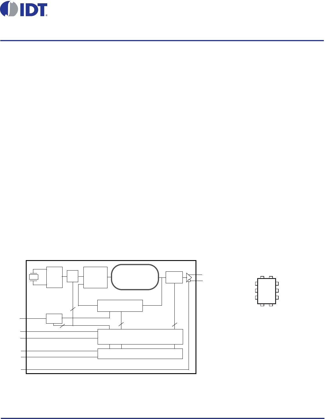
1
2
3
4
8
7
6
5
10 9
VC
OE
V
EE
VCC
nQ
Q
FSEL0
FSEL1
SCLK
SDATA
IDT8N3QV01 Rev G
10-lead Ceramic 5mm x 7mm x 1.55mm
package body
CD Package
Top View
Pin Assignment
Block Diagram
Q
nQ
OSC
114.285 MHz
÷MINT, MFRAC
PFD
&
LPF
FemtoClock® NG
VCO
1950-2600MHz
÷N
I
2
C Control
Configuration Register (ROM)
(Frequency, APR, Polarity)
25
7
VC
FSEL1
FSEL0
SCLK
SDATA
OE
Pulldown
Pulldown
Pullup
Pullup
Pullup
A/D
7
÷P
2