LTC4218
7
4218fh
For more information www.linear.com/LTC4218
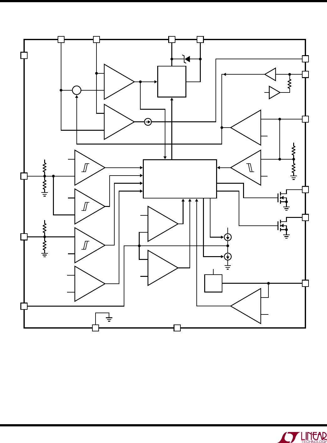
pin Functions
Exposed Pad: Exposed pad may be left open or connected
to device ground.
FB: Foldback and Power Good Comparator Input. Connect
this pin to an external resistive divider from SOURCE for
the LTC4218 (adjustable version). The LTC4218-12 version
uses a fixed internal divider with optional external adjust-
ment. Open the pin if the LTC4218-12 thresholds for 12V
operation are desired. If the voltage falls below 0.6V, the
output power is considered bad and the current limit is
reduced. If the voltage falls below 1.21V the PG pin will
pull low to indicate the power is bad.
F LT : Overcurrent Fault Indicator. Open drain output pulls
low when an overcurrent fault has occurred and the circuit
breaker trips. For overcurrent auto-retry tie to UV pin (see
Applications Information for details).
GATE: Gate Drive for External N-Channel FET. An internal
24µA current source charges the gate of the external
N-channel MOSFET. A resistor and capacitor network
from this pin to ground sets the turn-on rate. During an
undervoltage or overvoltage generated turn-off a 250µA
pull-down current turns the MOSFET off. During a short
circuit or undervoltage lockout, a 170mA pull-down current
source between GATE and SOURCE is activated.
GND: Device Ground.
I
MON
: Current Monitor Output. The current sourced from
this pin is defined as the current sense voltage (between
the SENSE
+
and SENSE
–
pins) multiplied by 6.67µA/mV.
Placing a 20k resistor from this pin to GND creates a 0V to
2V voltage swing when the current sense voltage ranges
from 0mV to 15mV.
INTV
CC
: Internal 3.1V Supply Decoupling Output. This pin
must have a 1µF or larger capacitor. Overloading this pin
can disrupt internal operation.
I
SET
: Current Limit Adjustment Pin. For 15mV current limit
threshold, open this pin. This pin is driven by a 20k resistor
in series with a voltage source. The pin voltage is used to
generate the current limit threshold. The internal 20k resistor
(R
ISET
) and an external resistor (R
SET
) between I
SET
and
ground create an attenuator that lowers the current limit
value. Due to circuit tolerance, the I
SET
resistor should not
be less than 2k.
NC: No Connection
OV: Overvoltage Comparator Input. Connect this pin to an
external resistive divider from V
DD
for the LTC4218 (adjust-
able version). The LTC4218-12 version uses a fixed internal
divider with optional external adjustment for 12V operation.
Open the
pin if the LTC4218-12 thresholds are desired. If
the voltage at this pin rises above 1.235V, an overvoltage
is detected and the switch turns off. Tie to GND if unused.
PG: Power Good Indicator. Open drain output pulls low
when the FB pin drops below 1.21V indicating the power
is bad. If the FB pin rises above 1.23V and the GATE to
SOURCE voltage exceeds 4.2V, the open-drain pull-down
releases the PG pin to go high.
SENSE
–
: Current Sense Minus Input. Connect this pin to
the opposite of V
DD
current sense resistor side. The cur-
rent limit circuit controls the GATE pin to limit the sense
voltage between the SENSE
+
and SENSE
–
pins to 15mV
or less depending on the voltage at the FB pin.
SENSE
+
: Current Sense Plus Input. Connect this pin to
the V
DD
side of the current sense resistor.
SOURCE: N-Channel MOSFET Source Connection. Connect
this pin to the source of the external N-channel MOSFET
switch. This pin provides a return for the gate pull-down
circuit. In the LTC4218-12 version, the power good com
-
parator monitors an internal resistive divider between the
SOURCE pin and GND.
TIMER:
T
imer Input. Connect a capacitor between this pin
and ground to set a 12ms/µF duration for current limit
before the switch is turned off. If the UV pin is toggled
low while the MOSFET switch is off, the switch will turn on
again following a cool down time of 518ms/µF duration.
UV: Undervoltage Comparator Input. Tie high if unused.
Connect this pin to an external resistive divider from V
DD
for the LTC4218 (adjustable version). The LTC4218-12
version drives the UV pin with an internal resistive divider
from V
DD
. Open the pin if the preset LTC4218-12 thresh-
olds for 12V operation are desired. If the UV pin voltage
falls below 1.15V, an under
voltage is detected and the
switch turns off. Pulling this pin below 0.62V resets the
overcurrent fault and allows the switch to turn back on
(see Applications Information for details). If overcurrent
auto-retry is desired then tie this pin to the F LT
pin.
V
DD
: Supply Voltage. This pin has an undervoltage lockout
threshold of 2.73V.