Important notice
Dear Customer,
On 7 February 2017 the former NXP Standard Product business became a new company with the
tradename Nexperia. Nexperia is an industry leading supplier of Discrete, Logic and PowerMOS
semiconductors with its focus on the automotive, industrial, computing, consumer and wearable
application markets
In data sheets and application notes which still contain NXP or Philips Semiconductors references, use
the references to Nexperia, as shown below.
Instead of http://www.nxp.com, http://www.philips.com/ or http://www.semiconductors.philips.com/,
use http://www.nexperia.com
Instead of sales.addresses@www.nxp.com or sales.addresses@www.semiconductors.philips.com, use
salesaddresses@nexperia.com (email)
Replace the copyright notice at the bottom of each page or elsewhere in the document, depending on
the version, as shown below:
- © NXP N.V. (year). All rights reserved or © Koninklijke Philips Electronics N.V. (year). All rights
reserved
Should be replaced with:
- © Nexperia B.V. (year). All rights reserved.
If you have any questions related to the data sheet, please contact our nearest sales office via e-mail
or telephone (details via salesaddresses@nexperia.com). Thank you for your cooperation and
understanding,
Kind regards,
Team Nexperia
1. General description
The 74CBTLV3126 provides a 4-bit high-speed bus switch with separate output enable
inputs (1OE to 4OE). The low on-state resistance of the switch allows connections to be
made with minimal propagation delay. The switch is disabled (high-impedance OFF-state)
when the output enable (nOE) input is LOW.
To ensure the high-impedance OFF-state during power-up or power-down, nOE should be
tied to the GND through a pull-down resistor. The minimum value of the resistor is
determined by the current-sinking capability of the driver.
Schmitt trigger action at control input makes the circuit tolerant to slower input rise and fall
times across the entire V
CC
range from 2.3 V to 3.6 V.
This device is fully specified for partial power-down applications using I
OFF
.
The I
OFF
circuitry disables the output, preventing the damaging backflow current through
the device when it is powered down.
2. Features and benefits
Supply voltage range from 2.3 V to 3.6 V
Standard ’126’-type pinout
High noise immunity
Complies with JEDEC standard:
JESD8-5 (2.3 V to 2.7 V)
JESD8-B/JESD36 (2.7 V to 3.6 V)
ESD protection:
HBM JESD22-A114F exceeds 2000 V
MM JESD22-A115-A exceeds 200 V
CDM AEC-Q100-011 revision B exceeds 1000 V
5 switch connection between two ports
Rail to rail switching on data I/O ports
CMOS low power consumption
Latch-up performance exceeds 250 mA per JESD78B Class I level A
I
OFF
circuitry provides partial Power-down mode operation
Multiple package options
Specified from 40 Cto+85C and 40 Cto+125C
74CBTLV3126
4-bit bus switch
Rev. 4 — 8 November 2016 Product data sheet
74CBTLV3126 All information provided in this document is subject to legal disclaimers. © NXP Semiconductors N.V. 2016. All rights reserved.
Product data sheet Rev. 4 — 8 November 2016 2 of 18
NXP Semiconductors
74CBTLV3126
4-bit bus switch
3. Ordering information
[1] Also known as QSOP16.
4. Functional diagram
Table 1. Ordering information
Type number Package
Temperature range Name Description Version
74CBTLV3126DS 40 C to +125 C SSOP16
[1]
plastic shrink small outline package; 16 leads;
body width 3.9 mm; lead pitch 0.635 mm
SOT519-1
74CBTLV3126PW 40 C to +125 C TSSOP14 plastic thin shrink small outline package; 14 leads;
body width 4.4 mm
SOT402-1
74CBTLV3126BQ 40 C to +125 C DHVQFN14 plastic dual in-line compatible thermal enhanced very
thin quad flat package; no leads; 14 terminals;
body 2.5 3 0.85 mm
SOT762-1
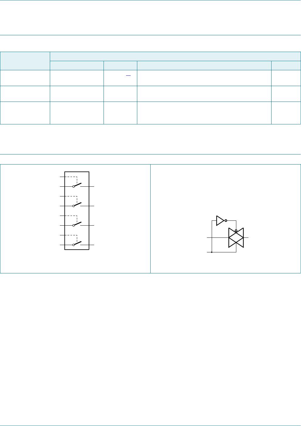
Fig 1. Logic symbol Fig 2. Logic diagram (one switch)
DDM
2(
$ %
2(
$ %
2(
$ %
2(
$ %
DDO
Q2(
Q$ Q%

74CBTLV3126DS,118

Mfr. #:
Manufacturer:
Nexperia
Description:
Digital Bus Switch ICs Single 60Ohms 3.6V
Lifecycle:
New from this manufacturer.
Delivery:
DHL FedEx Ups TNT EMS
Payment:
T/T Paypal Visa MoneyGram Western Union

Products related to this Datasheet