MPLAB
®
ICE 2000
DS51140J-page 8 2004 Microchip Technology Inc.
5.6 DVA16XP187
5.7 DVA16XP282, DVA16XP401,
DVA16XL441 and DVA16PQ441
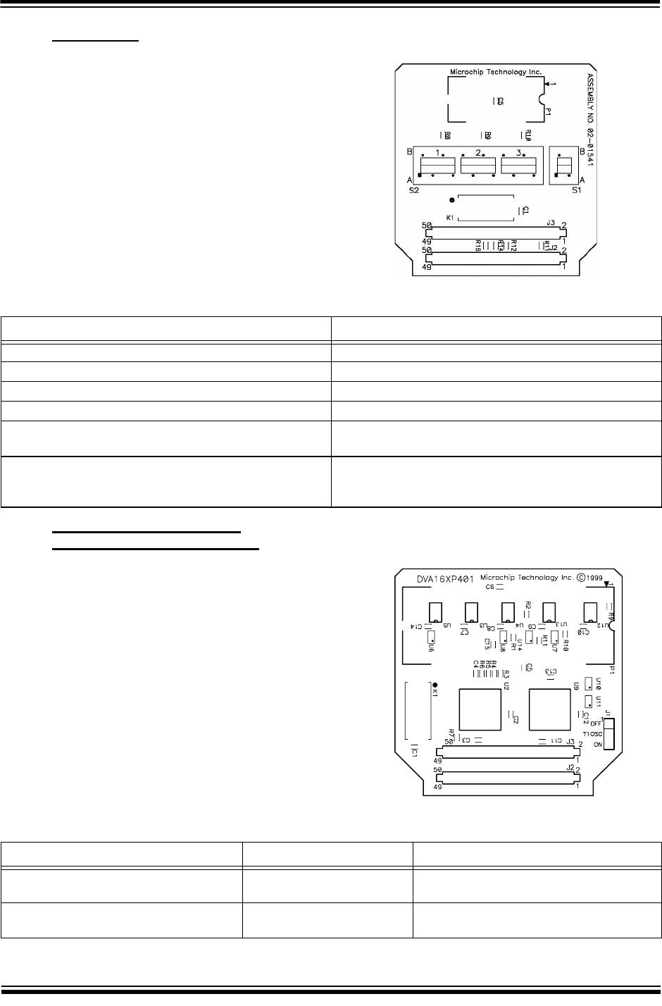
This device adapter is intended for use with PIC16F716
18-pin DIP devices. It has a second oscillator device that
allows TIMER1 oscillator input ranging from 32-40 kHz. It
has four mechanical switches. Target pins RB1 and RB2
can be routed to the emulator silicon on the PCM16YJ0
processor module or the TIMER1 oscillator device on the
device adapter. Target pin RB1 is routed to T1CKI. Target
pin RB3 can be a general purpose input or CCP1, as shown
in Table 5-5.
TABLE 5-6: DVA16XP187 DEVICE ADAPTER SWITCH ASSIGNMENT
Desired Function Switch Positions
RB1 Set S2-1 to position B
RB2 Set S2-2 to position B
RB3 Set S2-3 to position B
CCP1 Set S2-3 to position B
TIMER1 Clock Input Set S2-1 to position B and
set S1 to position B
TIMER1 Oscillator Input Set S2-1 to position A and
set S2-2 to position A and
set S1 to position A
These device adapters are intended for use with PICmicro
MCU devices supported by the PCM16XB0/B1,
PCM16XE0/E1, PCM16XK0 and the PCM16XL0 processor
modules. The device adapters have a second oscillator
device that allows TIMER1 oscillator input ranging from 32
to 40 kHz.
For PCM16XB0/B1, PCM16XE0/E1, PCM16XK0 and
PCM16XL0, configure jumper J1 per Table 5-7.
For all other processor modules supported by these device
adapters, leave the jumper on pins 1-2 (OFF); the Timer1
oscillator enable/disable function is software configurable.
TABLE 5-7: DVA16XP282, DVA16XP401, DVA16XL441 AND DVA16PQ441 JUMPER SETTINGS
Desired Function Switch Positions Results
TIMER1 Oscillator Input enabled Short J1 pins 2-3 (ON) RC0/T1OSO/T1CKI pin = T1OSO
RC1/T1OSI/CCP2 pin = T1OSI
TIMER1 Oscillator Input disabled Short J1 pins 1-2 (OFF) RC0/T1OSO/T1CKI pin = RC0 or T1CKI
RC1/T1OSI/CCP2 pin = RC1 or CCP2

