LT1126/LT1127
11267fa
3
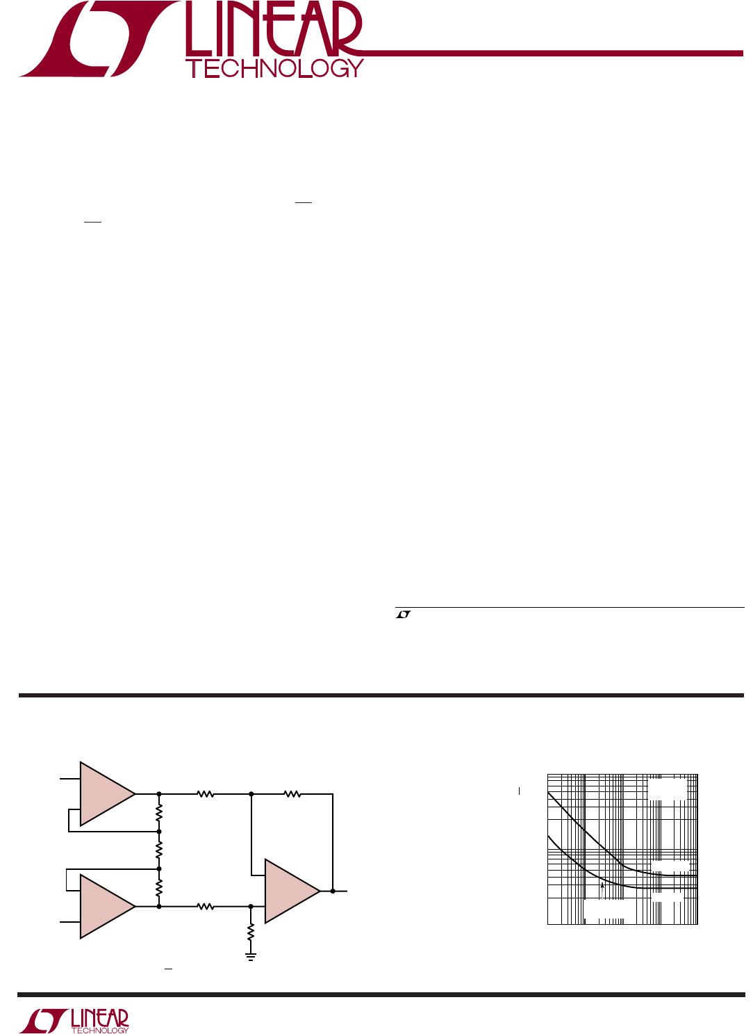
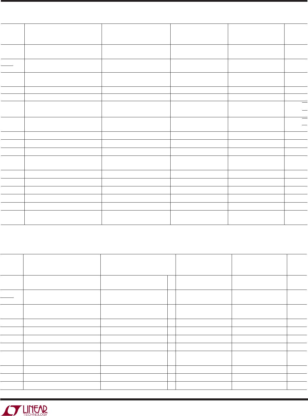
V
OS
Input Offset Voltage LT1126 20 70 25 100 µV
LT1127 25 90 30 140 µV
∆V
OS
Long Term Input Offset 0.3 0.3 µV/Mo
∆Time Voltage Stability
I
OS
Input Offset Current LT1126 5 15 6 20 nA
LT1127 6 20 7 30 nA
I
B
Input Bias Current ± 7 ± 20 ± 8 ± 30 nA
e
n
Input Noise Voltage 0.1Hz to 10Hz (Notes 8, 9) 70 200 70 nVp-p
Input Noise Voltage Density f
O
= 10Hz (Note 5) 3.0 5.5 3.0 5.5 nV/√Hz
f
O
= 1000Hz (Note 3) 2.7 4.2 2.7 4.2 nV/√Hz
i
n
Input Noise Current Density f
O
= 10Hz 1.3 1.3 pA/√Hz
f
O
= 1000Hz 0.3 0.3 pA/√Hz
V
CM
Input Voltage Range ± 12.0 ± 12.8 ± 12.0 ± 12.8 V
CMRR Common Mode Rejection Ratio V
CM
= ±12V 112 126 106 124 dB
PSRR Power Supply Rejection Ratio V
S
= ± 4V to ±18V 116 126 110 124 dB
A
VOL
Large Signal Voltage Gain R
L
≥ 10kΩ, V
O
= ±10V 5.0 17.0 3.0 15.0 V/µV
R
L
≥ 2kΩ, V
O
= ±10V 2.0 4.0 1.5 3.0 V/µV
V
OUT
Maximum Output Voltage Swing R
L
≥ 2kΩ ± 13.0 ± 13.8 ± 12.5 ± 13.8 V
SR Slew Rate R
L
≥ 2kΩ (Notes 3, 7) 8.0 11 8.0 11 V/µs
GBW Gain-Bandwidth Product f
O
= 10kHz (Note 3) 45 65 45 65 MHz
Z
O
Open Loop Output Resistance V
O
= 0, I
O
= 0 75 75 Ω
I
S
Supply Current Per Amplifier 2.6 3.1 2.6 3.1 mA
Channel Separation f ≤ 10Hz (Note 9) 134 150 130 150 dB
V
O
= ±10V, R
L
= 2kΩ
The ● denotes the specifications which apply over the full operating temperature range, otherwise specifications are at V
S
= ±15V,
− 55°C ≤ T
A
≤ 125°C, unless otherwise noted.
LT1126AM/AC LT1126M/C
LT1127AM/AC LT1127M/C
SYMBOL PARAMETER CONDITIONS (Note 2) MIN TYP MAX MIN TYP MAX UNITS
E
LECTR
IC
AL C CHARA TERIST
ICS
V
S
= ±15V, T
A
= 25°C, unless otherwise noted.
LT1126AM LT1126M
LT1127AM LT1127M
SYMBOL PARAMETER CONDITIONS (Note 1) MIN TYP MAX MIN TYP MAX UNITS
V
OS
Input Offset Voltage LT1126 ● 50 170 60 250 µV
LT1127 ● 55 190 70 290 µV
∆V
OS
Average Input Offset Voltage Drift (Note 5) ● 0.3 1.0 0.4 1.5 µV/°C
∆Temp
I
OS
Input Offset Current LT1126 ● 18 45 20 60 nA
LT1127 ● 18 55 20 70 nA
I
B
Input Bias Current ● ± 18 ± 55 ± 20 ± 70 nA
V
CM
Input Voltage Range ● ± 11.3 ± 12 ± 11.3 ± 12 V
CMRR Common Mode Rejection Ratio V
CM
= ±11.3V ● 106 122 100 120 dB
PSRR Power Supply Rejection Ratio V
S
= ± 4V to ±18V ● 110 122 104 120 dB
A
VOL
Large Signal Voltage Gain R
L
≥ 10kΩ, V
O
= ±10V ● 3.0 10.0 2.0 10.0 V/µV
R
L
≥ 2kΩ, V
O
= ±10V ● 1.0 3.0 0.7 2.0 V/µV
V
OUT
Maximum Output Voltage Swing R
L
≥ 2kΩ ● ± 12.5 ± 13.6 ± 12.0 ± 13.6 V
SR Slew Rate R
L
≥ 2kΩ (Notes 3, 7) ● 7.2 10 7.0 10 V/µs
I
S
Supply Current Per Amplifier ● 2.8 3.5 2.8 3.5 mA