Functional Block Diagram
Figure 3: Functional Block Diagram
DQ
DQ
DQ
DQ
DQ
DQ
DQ
DQ
ZQ
DQ0
DQ1
DQ2
DQ3
DQ4
DQ5
DQ6
DQ7
U1
DM CS# DQS DQS#
DQ
DQ
DQ
DQ
DQ
DQ
DQ
DQ
ZQ
DQ32
DQ33
DQ34
DQ35
DQ36
DQ37
DQ38
DQ39
U5
DM CS# DQS DQS#
DQ
DQ
DQ
DQ
DQ
DQ
DQ
DQ
ZQ
DQ8
DQ9
DQ10
DQ11
DQ12
DQ13
DQ14
DQ15
U2
DM CS# DQS DQS#
DQ
DQ
DQ
DQ
DQ
DQ
DQ
DQ
ZQ
DQ16
DQ17
DQ18
DQ19
DQ20
DQ21
DQ22
DQ23
U3
DM CS# DQS DQS#
DQ
DQ
DQ
DQ
DQ
DQ
DQ
DQ
ZQ
DQ24
DQ25
DQ26
DQ27
DQ28
DQ29
DQ30
DQ31
U4
DM CS# DQS DQS#
DQ
DQ
DQ
DQ
DQ
DQ
DQ
DQ
ZQ
DQ40
DQ41
DQ42
DQ43
DQ44
DQ45
DQ46
DQ47
U6
DM CS# DQS DQS#
DQ
DQ
DQ
DQ
DQ
DQ
DQ
DQ
ZQ
DQ48
DQ49
DQ50
DQ51
DQ52
DQ53
DQ54
DQ55
U7
DM CS# DQS DQS#
DQ
DQ
DQ
DQ
DQ
DQ
DQ
DQ
ZQ
DQ56
DQ57
DQ58
DQ59
DQ60
DQ61
DQ62
DQ63
U8
DM CS# DQS DQS#
DQS0#
DQS0
DM0
S0#
DQS1#
DQS1
DM1
DQS2#
DQS2
DM2
DQS3#
DQS3
DM3
DQS4#
DQS4
DM4
DQS5#
DQS5
DM5
DQS6#
DQS6
DM6
DQS7#
DQS7
DM7
BA[2:0]
A[15/14/13:0]
RAS#
CAS#
WE#
CKE0
ODT0
RESET#
BA[2:0]: DDR3 SDRAM
A[15/14/13:0]: DDR3 SDRAM
RAS#: DDR3 SDRAM
CAS#: DDR3 SDRAM
WE#: DDR3 SDRAM
CKE0: DDR3 SDRAM
ODT0: DDR3 SDRAM
RESET#: DDR3 SDRAM
DDR3 SDRAM x8
CK0
CK0#
A0
SPD EEPROM
A1
A2
SA0 SA1
SDA
SCL
WP
U9
V
REFCA
V
SS
DDR3 SDRAM
DDR3 SDRAM
V
DD
Address, command,
and control termination
V
DDSPD
SPD EEPROM
V
TT
DDR3 SDRAM
DDR3 SDRAM
V
REFDQ
V
SS
Address, command, control, and clock line terminations:
CKE0, A[15/14/13:0],
RAS#, CAS#, WE#,
S0#, ODT0, BA[2:0]
CK0
CK0#
SA2
V
SS
V
SS
V
SS
V
SS
V
SS
V
SS
V
SS
V
SS
DDR3
SDRAM
V
TT
DDR3
SDRAM
V
DD
CK1
CK1#
Unused clock termination
Note:
1. The ZQ ball on each DDR3 component is connected to an external 240Ω ±1% resistor
that is tied to ground. It is used for the calibration of the component’s ODT and output
driver.
1GB, 2GB, 4GB (x64, SR) 240-Pin 1.35V DDR3L UDIMM
Functional Block Diagram
PDF: 09005aef8413b5fe
ktf8c128_256_512x64az.pdf – Rev. K 9/15 EN
7
Micron Technology, Inc. reserves the right to change products or specifications without notice.
© 2010 Micron Technology, Inc. All rights reserved.
General Description
DDR3 SDRAM modules are high-speed, CMOS dynamic random access memory mod-
ules that use internally configured 8-bank DDR3 SDRAM devices. DDR3 SDRAM mod-
ules use DDR architecture to achieve high-speed operation. DDR3 architecture is essen-
tially an 8n-prefetch architecture with an interface designed to transfer two data words
per clock cycle at the I/O pins. A single read or write access for the DDR3 SDRAM mod-
ule effectively consists of a single 8n-bit-wide, one-clock-cycle data transfer at the inter-
nal DRAM core and eight corresponding n-bit-wide, one-half-clock-cycle data transfers
at the I/O pins.
DDR3 modules use two sets of differential signals: DQS, DQS# to capture data and CK
and CK# to capture commands, addresses, and control signals. Differential clocks and
data strobes ensure exceptional noise immunity for these signals and provide precise
crossing points to capture input signals.
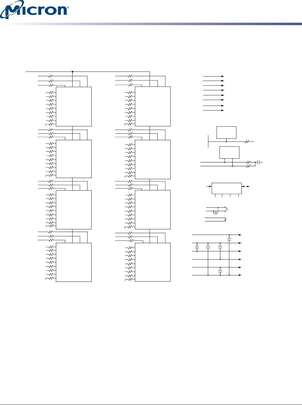
Fly-By Topology
DDR3 modules use faster clock speeds than earlier DDR technologies, making signal
quality more important than ever. For improved signal quality, the clock, control, com-
mand, and address buses have been routed in a fly-by topology, where each clock, con-
trol, command, and address pin on each DRAM is connected to a single trace and ter-
minated (rather than a tree structure, where the termination is off the module near the
connector). Inherent to fly-by topology, the timing skew between the clock and DQS sig-
nals can be easily accounted for by using the write-leveling feature of DDR3.
Serial Presence-Detect EEPROM Operation
DDR3 SDRAM modules incorporate serial presence-detect. The SPD data is stored in a
256-byte EEPROM. The first 128 bytes are programmed by Micron to comply with
JEDEC standard JC-45, "Appendix X: Serial Presence Detect (SPD) for DDR3 SDRAM
Modules." These bytes identify module-specific timing parameters, configuration infor-
mation, and physical attributes. The remaining 128 bytes of storage are available for use
by the customer. System READ/WRITE operations between the master (system logic)
and the slave EEPROM device occur via a standard I
2
C bus using the DIMM’s SCL
(clock) SDA (data), and SA (address) pins. Write protect (WP) is connected to V
SS
, per-
manently disabling hardware write protection. For further information refer to Micron
technical note TN-04-42, "Memory Module Serial Presence-Detect."
1GB, 2GB, 4GB (x64, SR) 240-Pin 1.35V DDR3L UDIMM
General Description
PDF: 09005aef8413b5fe
ktf8c128_256_512x64az.pdf – Rev. K 9/15 EN
8
Micron Technology, Inc. reserves the right to change products or specifications without notice.
© 2010 Micron Technology, Inc. All rights reserved.
Electrical Specifications
Stresses greater than those listed may cause permanent damage to the module. This is a
stress rating only, and functional operation of the module at these or any other condi-
tions outside those indicated in each device's data sheet is not implied. Exposure to ab-
solute maximum rating conditions for extended periods may adversely affect reliability.
Table 9: Absolute Maximum Ratings
Symbol Parameter Min Max Units
V
DD
V
DD
supply voltage relative to V
SS
–0.4 1.975 V
V
IN
, V
OUT
Voltage on any pin relative to V
SS
–0.4 1.975 V
Table 10: Operating Conditions
Symbol Parameter Min Nom Max Units Notes
V
DD
V
DD
supply voltage 1.283 1.35 1.45 V
1.425 1.5 1.575 V 1
I
VTT
Termination reference current from V
TT
–600 600 mA
V
TT
Termination reference voltage (DC)
– command/address bus
0.49 × V
DD
- 20mV 0.5 × V
DD
0.51 × V
DD
+ 20mV V 2
I
I
Input leakage current;
Any input 0V V
IN
V
DD
;
V
REF
input 0V V
IN
0.95V
(All other pins not under test
= 0V)
Address in-
puts, RAS#,
CAS#, WE#,
BA, S#, CKE,
ODT, CK,
CK#
–16 0 16 µA
DM –2 0 2
I
OZ
Output leakage current;
0V V
OUT
V
DDQ
; DQ and
ODT are disabled; ODT is HIGH
DQ, DQS,
DQS#
–5 0 5 µA
I
VREF
V
REF
supply leakage current; V
REFDQ
= V
DD
/2
or V
REFCA
= V
DD
/2 (All other pins not under
test = 0V.)
–8 0 8 µA
T
A
Module ambient operating
temperature
Commercial 0 70 °C 3, 4
T
C
DDR3 SDRAM component case
operating temperature
Commercial 0 95 °C 3, 4, 5
Notes:
1. Module is backward-compatible with 1.5V operation. Refer to device specification for
details and operation guidance.
2. V
TT
termination voltage in excess of the stated limit will adversely affect the command
and address signals’ voltage margin and will reduce timing margins.
3. T
A
and T
C
are simultaneous requirements.
4. For further information, refer to technical note TN-00-08: ”Thermal Applications,” avail-
able on Micron’s Web site.
5. The refresh rate is required to double when 85°C < T
C
95°C.
1GB, 2GB, 4GB (x64, SR) 240-Pin 1.35V DDR3L UDIMM
Electrical Specifications
PDF: 09005aef8413b5fe
ktf8c128_256_512x64az.pdf – Rev. K 9/15 EN
9
Micron Technology, Inc. reserves the right to change products or specifications without notice.
© 2010 Micron Technology, Inc. All rights reserved.

MT8KTF12864AZ-1G1G1

Mfr. #:
Manufacturer:
Micron
Description:
MODULE DDR3L SDRAM 1GB 240UDIMM
Lifecycle:
New from this manufacturer.
Delivery:
DHL FedEx Ups TNT EMS
Payment:
T/T Paypal Visa MoneyGram Western Union