74FCT162374ETPAG

4
INDUSTRIAL TEMPERATURE RANGE
IDT74FCT162374AT/CT/ET
FAST CMOS 16-BIT REGISTER (3-STATE)
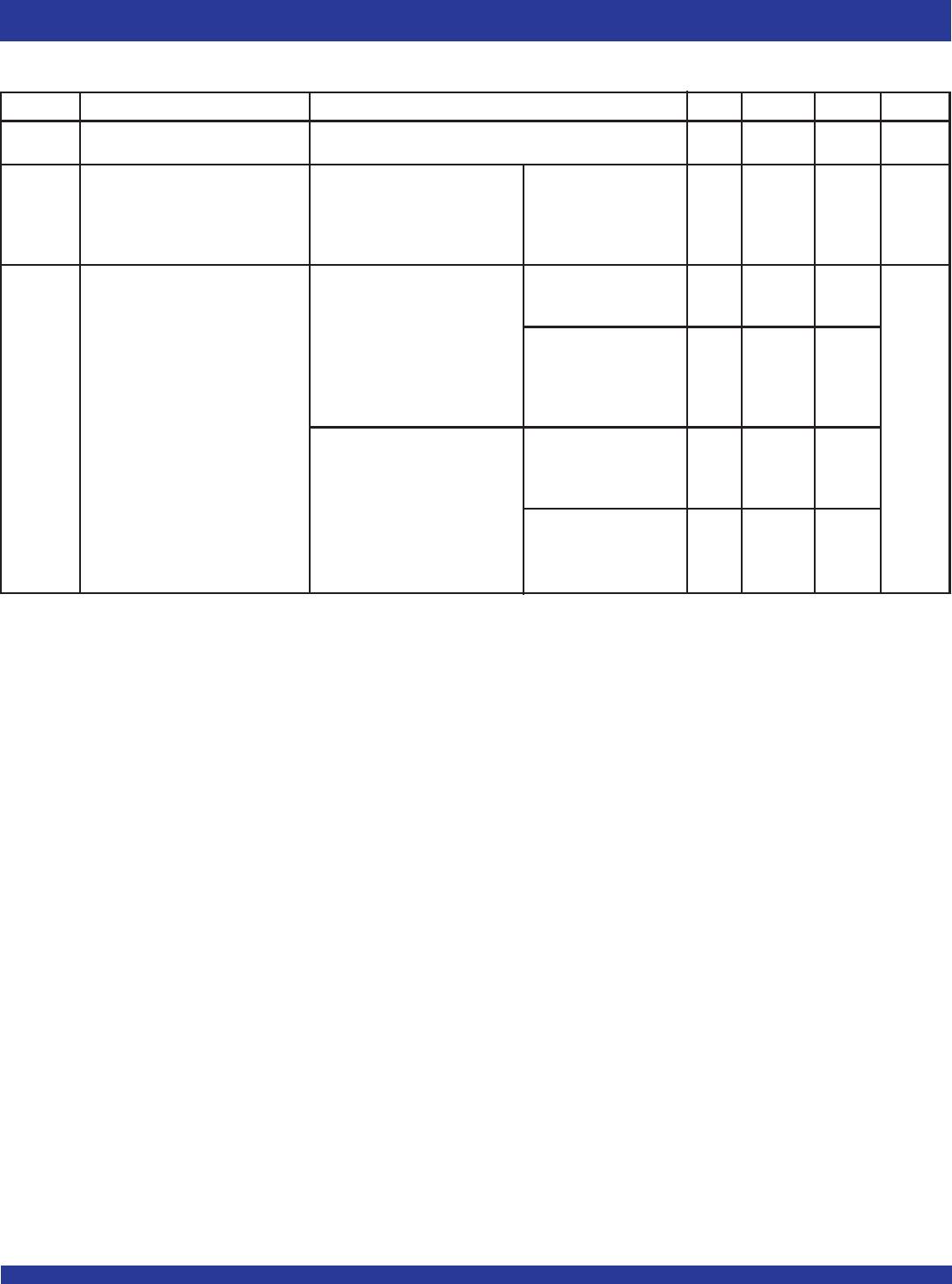
Symbol Parameter Test Conditions
(1)
Min. Typ.
(2)
Max. Unit
ΔI
CC Quiescent Power Supply Current VCC = Max. 0.5 1.5 mA
TTL Inputs HIGH VIN = 3.4V
(3)
ICCD Dynamic Power Supply VCC = Max. VIN = VCC 60 100 µ A /
Current
(4)
Outputs Open VIN = GND MHz
xOE = GND
One Input Togging
50% Duty Cycle
I
C Total Power Supply Current
(6)
VCC = Max. VIN = VCC 0.6 1.5 mA
Outputs Open V
IN = GND
fCP = 10MHz
50% Duty Cycle V
IN = 3.4V 1.1 3
xOE = GND V
IN = GND
fi = 5MHz
50% Duty Cycle
One Bit Toggling
V
CC = Max. VIN = VCC 3 5.5
(5)
Outputs Open VIN = GND
fCP = 10MHz
50% Duty Cycle
xOE = GND V
IN = 3.4V 7.5 19
(5)
Sixteen BitsTogging VIN = GND
fi = 2.5MHz
50% Duty Cycle
POWER SUPPLY CHARACTERISTICS
NOTES:
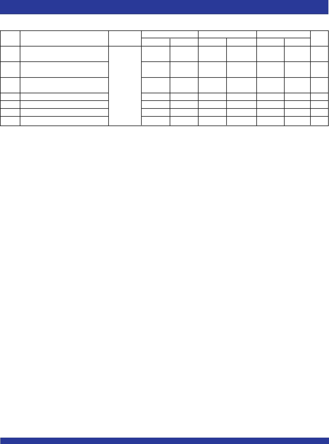
1. For conditions shown as Min. or Max., use appropriate value specified under Electrical Characteristics for the applicable device type.
2. Typical values are at VCC = 5.0V, +25°C ambient.
3. Per TTL driven input (VIN = 3.4V). All other inputs at VCC or GND.
4. This parameter is not directly testable, but is derived for use in Total Power Supply Calculations.
5. Values for these conditions are examples of the ICC formula. These limits are guaranteed but not tested.
6. IC = IQUIESCENT + IINPUTS + IDYNAMIC
IC = ICC + ΔICC DHNT + ICCD (fCPNCP/2 + fiNi)
ICC = Quiescent Current (ICCL, ICCH and ICCZ)
ΔICC = Power Supply Current for a TTL High Input (VIN = 3.4V)
DH = Duty Cycle for TTL Inputs High
NT = Number of TTL Inputs at DH
ICCD = Dynamic Current caused by an Input Transition Pair (HLH or LHL)
fCP = Clock Frequency for Register Devices (Zero for Non-Register Devices)
NCP = Number of Clock Inputs at fCP
fi = Input Frequency
Ni = Number of Inputs at fi
5
IDT74FCT162374AT/CT/ET
FAST CMOS 16-BIT REGISTER (3-STATE)
INDUSTRIAL TEMPERATURE RANGE
74FCT162374AT 74FCT162374CT 74FCT162374ET
Symbol Parameter Condition
(1)
Min.
(2)
Max. Min.
(2)
Max. Min.
(2)
Max. Unit
t
PLH Propagation Delay CL = 50pF 2 6.5 2 5.2 1.5 3.7 ns
tPHL xCLK to xOx RL = 500Ω
t
PZH Output Enable Time 1.5 6.5 1.5 5.5 1.5 4.4 ns
tPZL
tPHZ Output Disable Time 1.5 5.5 1.5 5 1.5 3.6 ns
tPLZ
tSU Set-up Time HIGH or LOW, xDx to xCLK 2 2 1.5 ns
tH Hold Time HIGH or LOW, xDx to xCLK 1.5 1.5 0 ns
tW xCLK Pulse Width HIGH or LOW 5 5 3
(4)
—ns
t
SK(o) Output Skew
(3)
0.5 0.5 0.5 ns
SWITCHING CHARACTERISTICS OVER OPERATING RANGE
NOTES:
1. See test circuit and waveforms.
2. Minimum limits are guaranteed but not tested on Propagation Delays.
3. Skew between any two outputs of the same package switching in the same direction. This parameter is guaranteed by design.
4. This limit is guaranteed but not tested.
6
INDUSTRIAL TEMPERATURE RANGE
IDT74FCT162374AT/CT/ET
FAST CMOS 16-BIT REGISTER (3-STATE)
Pulse
Generator
R
T
D.U.T.
V
CC
V
IN
C
L
V
OUT
50pF
500Ω
500Ω
7.0V
3V
1.5V
0V
3V
1.5V
0V
3V
1.5V
0V
3V
1.5V
0V
DATA
INPUT
TIMING
INPUT
ASYNCHRONOUS CONTROL
PRESET
CLEAR
ETC.
SYNCHRONOUS CONTROL
t
SU
t
H
t
REM
t
SU
t
H
PRESET
CLEAR
CLOCK ENABLE
ETC.
HIGH-LOW-HIGH
PULSE
LOW-HIGH-LOW
PULSE
t
W
1.5V
1.5V
SAME PHASE
INPUT TRANSITION
3V
1.5V
0V
1.5V
V
OH
t
PLH
OUTPUT
OPPOSITE PHASE
INPUT TRANSITION
3V
1.5V
0V
t
PLH
t
PHL
t
PHL
V
OL
CONTROL
INPUT
3V
1.5V
0V
3.5V
0V
OUTPUT
NORMALLY
LOW
OUTPUT
NORMALLY
HIGH
SWITCH
CLOSED
SWITCH
OPEN
V
OL
0.3V
0.3V
t
PLZ
t
PZL
t
PZH
t
PHZ
3.5V
0V
1.5V
1.5V
ENABLE DISABLE
V
OH
TEST CIRCUITS AND WAVEFORMS
Propagation Delay
Test Circuit for All Outputs
Enable and Disable Times
Set-up, Hold and Release Times
Pulse Width
Test Switch
Open Drain
Disable Low Closed
Enable Low
All Other Tests Open
SWITCH POSITION
DEFINITIONS:
CL = Load capacitance: includes jig and probe capacitance.
R
T = Termination resistance: should be equal to ZOUT of the Pulse Generator.
NOTES:
1. Diagram shown for input Control Enable-LOW and input Control Disable-HIGH.
2. Pulse Generator for All Pulses: Rate 1.0MHz; t
F 2.5ns; tR 2.5ns.

74FCT162374ETPAG

Mfr. #:
Manufacturer:
IDT
Description:
Registers 16-Bit Register
Lifecycle:
New from this manufacturer.
Delivery:
DHL FedEx Ups TNT EMS
Payment:
T/T Paypal Visa MoneyGram Western Union