MAX4501/MAX4502
Low-Voltage, SPST, CMOS Analog Switches
6 _______________________________________________________________________________________
Applications Information
Power-Supply Considerations
The MAX4501/MAX4502 are constructed like most
CMOS analog switches, except they have only two sup-
ply pins: V+ and GND. V+ and GND drive the internal
CMOS switches and set the analog voltage limits of the
switch. Reverse ESD-protection diodes are internally
connected between each analog signal pin and both
V+ and GND. One of these diodes conducts if any ana-
log signal exceeds V+ or GND. During normal opera-
tion, these and other reverse-biased ESD diodes leak,
forming the only current drawn from V+ or GND.
Virtually all the analog leakage current comes from the
ESD diodes. Although the ESD diodes on a given sig-
nal pin are identical and therefore fairly well balanced,
they are reverse biased differently. Each is biased by
either V+ or GND and the analog signal. This means
their leakages will vary as the signal varies. The differ-
ence in the two diode leakages to the V+ and GND
pins constitutes the analog signal-path leakage current.
All analog leakage current flows between each pin and
one of the supply terminals, not to the other switch ter-
minal. This is why both sides of a given switch can
show leakage currents of the same or opposite polarity.
There is no connection between the analog-signal
paths and V+ or GND.
V+ and GND also power the internal logic and logic-
level translators, and set the input logic limits. The
logic-level translators convert the logic levels to
switched V+ and GND signals to drive the analog sig-
nal gates. This drive signal is the only connection
between the logic supplies (and signals) and the ana-
log supplies. COM, NO, and NC pins have ESD-protec-
tion diodes to V+ and GND.
The logic-level thresholds are CMOS/TTL compatible
when V+ is +5V. As V+ rises, the threshold increases
slightly. When V+ reaches +12V, the logic-level thresh-
old is about 3V—above the TTL guaranteed high-level
minimum of 2.8V, but still compatible with CMOS out-
puts.
Do not connect the MAX4501/MAX4502’s V+ pin to
+3V and then connect the logic-level pins to TTL
logic-level signals. TTL levels can exceed +3V and
violate the absolute maximum ratings, damaging
the part and/or external circuits.
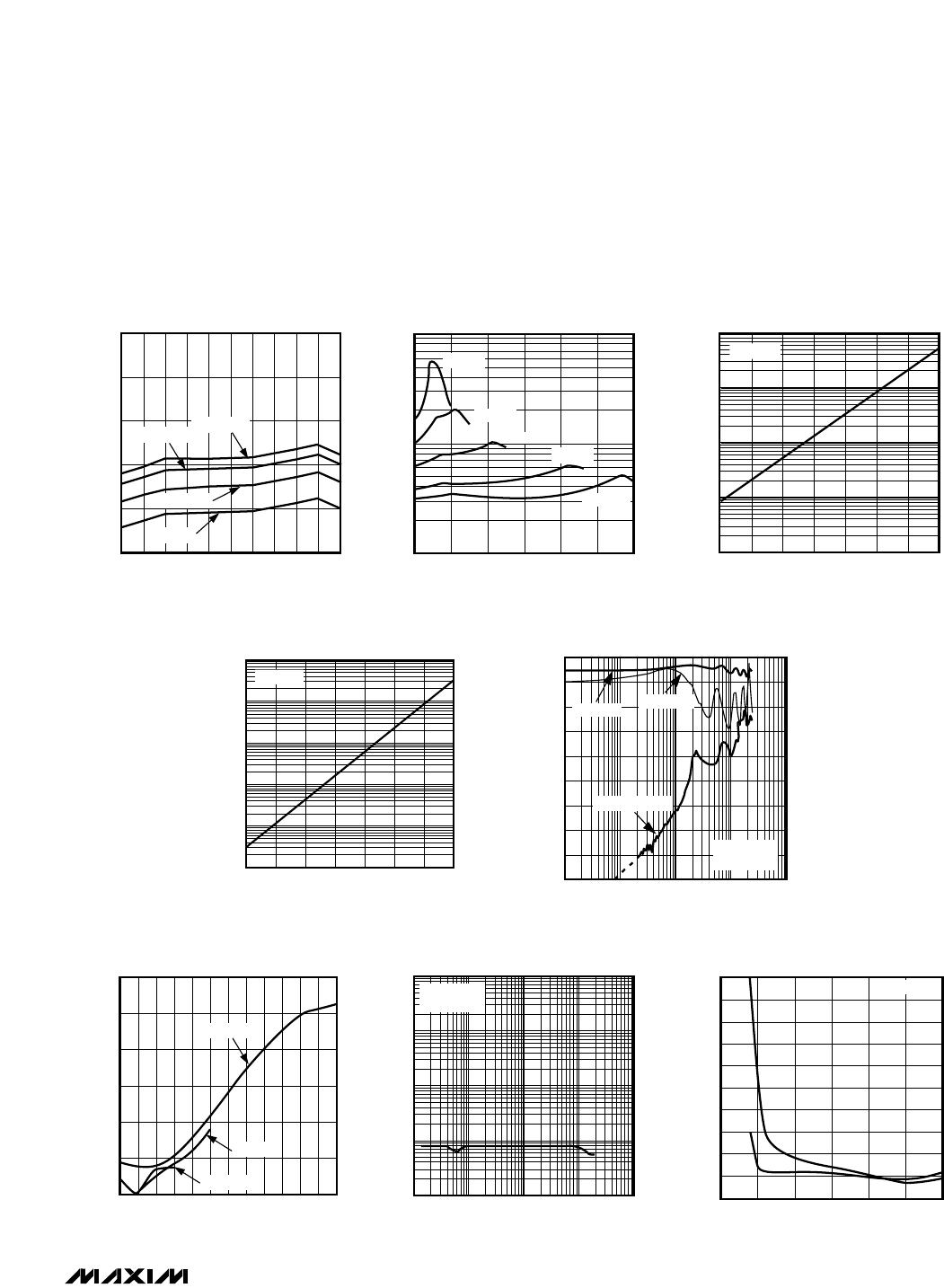
High-Frequency Performance
In 50Ω systems, signal response is reasonably flat up
to 250MHz (see Typical Operating Characteristics).
Above 20MHz, the on-response has several minor
peaks that are highly layout dependent. The problem is
not in turning the switch on; it’s in turning it off. The off-
state switch acts like a capacitor and passes higher
frequencies with less attenuation. At 10MHz, off-isola-
tion is about -60dB in 50Ω systems, decreasing
approximately 20dB per decade as frequency increas-
es. Higher circuit impedances also cause off-isolation
to decrease. Adjacent channel attenuation is about 3dB
above that of a bare IC socket, and is due entirely to
capacitive coupling.
______________________________________________________________Pin Description
Note: NO, NC, and COM pins are identical and interchangeable. Any may be considered as an input or an output; signals pass
equally well in both directions.
FUNCTIONNAME
MAX4501 MAX4502
SO/DIP
SC70-5/SOT23-5
SO/DIP
SC70-5/SOT23-5
Positive Supply-Voltage Input (analog and digital)
PIN
1 1 1 1 COM Analog Switch Common Terminal
2, 3, 5 — 2, 3, 5 — N.C. No Connection. Not internally connected.
4 5 V+
6 4 6 4 IN Digital Control Input
7 3 7 3 GND Ground
8 2 — — NO Analog Switch (normally open)
— — 8 2 NC Analog Switch (normally closed)
54