VNP35N07
"OMNIFET":
FULLY AUTOPROTECTED POWER MOSFET
March 2004
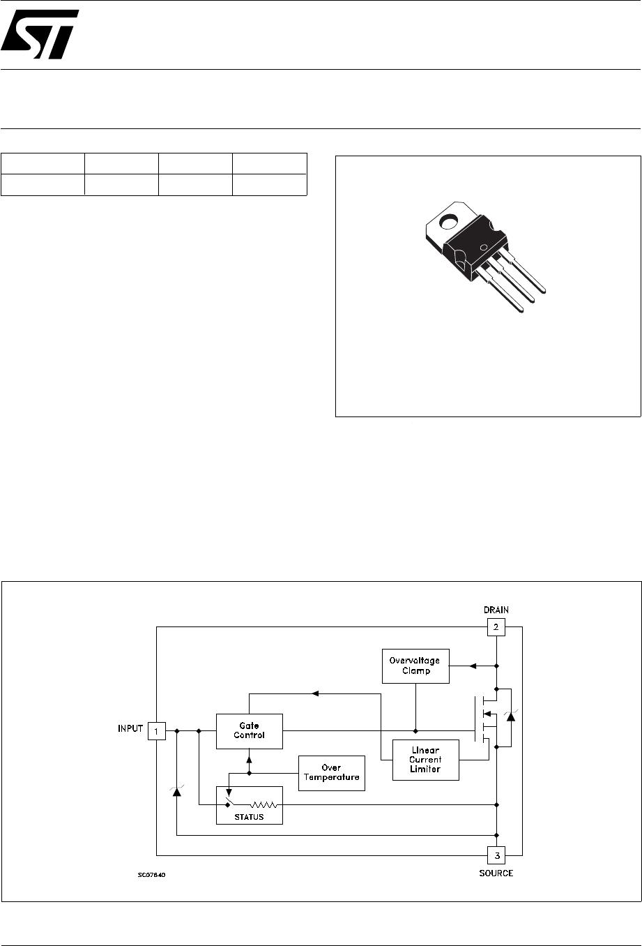
1
2
3
TO-220
BLOCK DIAGRAM
TYPE V
clamp
R
DS(on)
I
lim
VNP35N07 70 V 0.028 Ω 35 A
■ LINEAR CURRENT LIMITATION
■ THERMAL SHUT DOWN
■ SHORT CIRCUIT PROTECTION
■ INTEGRATED CLAMP
■ LOW CURRENT DRAWN FROM INPUT PIN
■ DIAGNOSTIC FEEDBACK THROUGH INPUT
PIN
■ ESD PROTECTION
■ DIRECT ACCESS TO THE GATE OF THE
POWER MOSFET (ANALOG DRIVING)
■ COMPATIBLE WITH STANDARD POWER
MOSFET
■ STANDARD TO-220 PACKAGE
DESCRIPTION
The VNP35N07 is a monolithic device made
using STMicroelectronics VIPower Technology,
intended for replacement of standard power
MOSFETS in DC to 50 KHz applications.
Built-in thermal shut-down, linear current limi-
tation and overvoltage clamp protect the chip
in harsh enviroments.
Fault feedback can be detected by monitoring the
voltage at the input pin.
1/11
Obsolete Product(s) - Obsolete Product(s)