IPZ40N04S53R1ATMA1

IPZ40N04S5-3R1
OptiMOS
-5 Power-Transistor
Features
• OptiMOS - power MOSFET for automotive applications
• N-channel - Enhancement mode - Normal Level
• AEC Q101 qualified
• MSL1 up to 260°C peak reflow
• 175°C operating temperature
• Green Product (RoHS compliant)
• 100% Avalanche tested
Maximum ratings, at T
j
=25 °C, unless otherwise specified
Parameter Symbol Conditions Unit
Continuous drain current
1)
I
D
T
C
=25°C, V
GS
=10V
40 A
T
C
=100°C, V
GS
=10V
2)
40
Pulsed drain current
2)
I
D,pulse
T
C
=25°C
160
Avalanche energy, single pulse
2)
E
AS
I
D
=20A
140 mJ
Avalanche current, single pulse
I
AS
-
40 A
Gate source voltage
V
GS
- ±20 V
Power dissipation
P
tot
T
C
=25°C
71 W
Operating and storage temperature
T
j
, T
stg
- -55 ... +175 °C
Value
V
DS
40 V
R
DS(on),max
3.1
mW
I
D
40 A
Product Summary
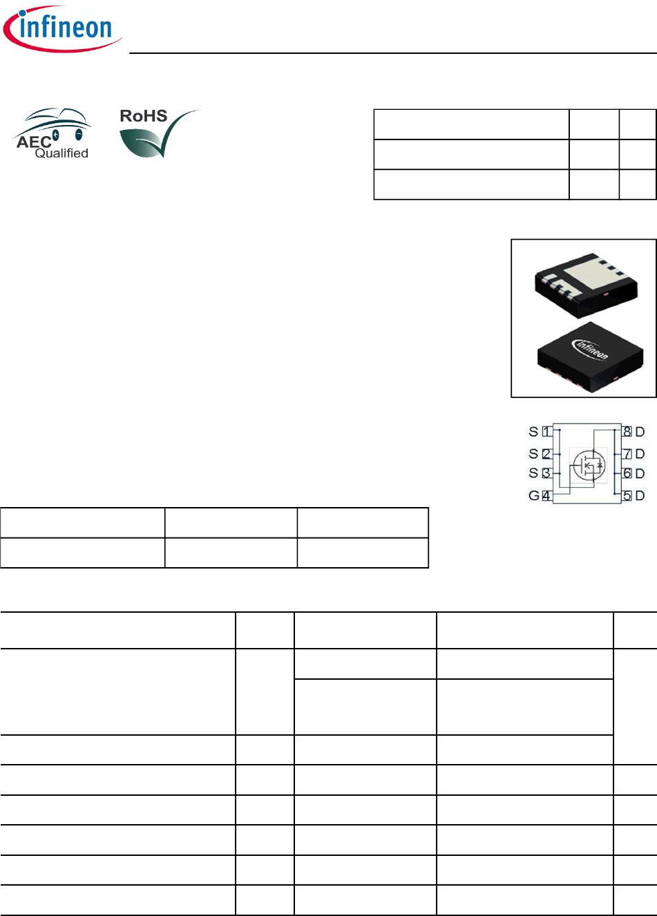
PG-TSDSON-8-33
Type Package Marking
IPZ40N04S5-3R1 PG-TSDSON-8-33 5N0431
1
1
Rev. 1.1
page 1 2015-07-27
IPZ40N04S5-3R1
Parameter Symbol Conditions Unit
min. typ. max.
Thermal characteristics
2)
Thermal resistance, junction - case
R
thJC
- - - 2.1 K/W
Thermal resistance, junction -
ambient
R
thJA
6 cm
2
cooling area
3)
- - 60
Electrical characteristics, at T
j
=25 °C, unless otherwise specified
Static characteristics
Drain-source breakdown voltage
V
(BR)DSS
V
GS
=0V, I
D
= 1mA
40 - - V
Gate threshold voltage
V
GS(th)
V
DS
=V
GS
, I
D
=30µA
2.2 2.8 3.4
Zero gate voltage drain current
I
DSS
V
DS
=40V, V
GS
=0V,
T
j
=25°C
- - 1 µA
V
DS
=40V, V
GS
=0V,
T
j
=125°C
2)
- - 100
Gate-source leakage current
I
GSS
V
GS
=20V, V
DS
=0V
- - 100 nA
Drain-source on-state resistance
R
DS(on)
V
GS
=7V, I
D
=20A
- 3.0 3.6
mW
V
GS
=10V, I
D
=20A
- 2.5 3.1
Values
Rev. 1.1
page 2 2015-07-27
IPZ40N04S5-3R1
Parameter Symbol Conditions Unit
min. typ. max.
Dynamic characteristics
2)
Input capacitance
C
iss
- 1740 2310 pF
Output capacitance
C
oss
- 490 650
Reverse transfer capacitance
C
rss
- 35 55
Turn-on delay time
t
d(on)
- 6 - ns
Rise time
t
r
- 3 -
Turn-off delay time
t
d(off)
- 11 -
Fall time
t
f
- 7 -
Gate Charge Characteristics
2)
Gate to source charge
Q
gs
- 7.7 10.2 nC
Gate to drain charge
Q
gd
- 7.1 10.6
Gate charge total
Q
g
- 31 41
Gate plateau voltage
V
plateau
- 4.4 - V
Reverse Diode
Diode continous forward current
2)
I
S
- - 40 A
Diode pulse current
1)
I
S,pulse
- - 160
Diode forward voltage
V
SD
V
GS
=0V, I
F
=20A,
T
j
=25°C
- 0.8 1.1 V
Reverse recovery time
1)
t
rr
V
R
=20V, I
F
=40A,
di
F
/dt=100A/µs
- 40 - ns
Reverse recovery charge
1)
Q
rr
- 30 - nC
3)
Device on 40 mm x 40 mm x 1.5 mm epoxy PCB FR4 with 6 cm
2
(one layer, 70 µm thick) copper area for drain
connection. PCB is vertical in still air.
1)
Current is limited by package; with an R
thJC
= 2.1K/W the chip is able to carry 112A at 25°C.
T
C
=25°C
2)
The parameter is not subject to production test- verified by design/characterization.
Values
V
GS
=0V, V
DS
=25V,
f=1MHz
V
DD
=20V, V
GS
=10V,
I
D
=40A, R
G
=3.5W
V
DD
=32V, I
D
=40A,
V
GS
=0 to 10V
Rev. 1.1
page 3 2015-07-27

IPZ40N04S53R1ATMA1

Mfr. #:
Manufacturer:
Infineon Technologies
Description:
MOSFET N-CHANNEL_30/40V
Lifecycle:
New from this manufacturer.
Delivery:
DHL FedEx Ups TNT EMS
Payment:
T/T Paypal Visa MoneyGram Western Union

Products related to this Datasheet