Document Number: 91116 www.vishay.com
S11-1053-Rev. C, 30-May-11 7
This document is subject to change without notice.
THE PRODUCTS DESCRIBED HEREIN AND THIS DOCUMENT ARE SUBJECT TO SPECIFIC DISCLAIMERS, SET FORTH AT
www.vishay.com/doc?91000
IRFBC40S, SiHFBC40S, IRFBC40L, SiHFBC40L
Vishay Siliconix
Fig. 14 - For N-Channel
Vishay Siliconix maintains worldwide manufacturing capability. Products may be manufactured at one of several qualified locations. Reliability data for Silicon
Technology and Package Reliability represent a composite of all qualified locations. For related documents such as package/tape drawings, part marking, and
reliability data, see www.vishay.com/ppg?91116
.
P.W.
Period
dI/dt
Diode recovery
dV/dt
Ripple 5 %
Body diode forward drop
Re-applied
voltage
Reverse
recovery
current
Body diode forward
current
V
GS
= 10 V
a
I
SD
Driver gate drive
D.U.T. l
SD
waveform
D.U.T. V
DS
waveform
Inductor current
D =
P.W.
Period
+
-
+
+
+
-
-
-
Peak Diode Recovery dV/dt Test Circuit
V
DD
dV/dt controlled by R
g
Driver same type as D.U.T.
I
SD
controlled by duty factor “D”
D.U.T. - device under test
D.U.T.
Circuit layout considerations
Low stray inductance
Ground plane
Low leakage inductance
current transformer
R
g
Note
a. V
GS
= 5 V for logic level devices
V
DD
Document Number: 91364 www.vishay.com
Revision: 15-Sep-08 1
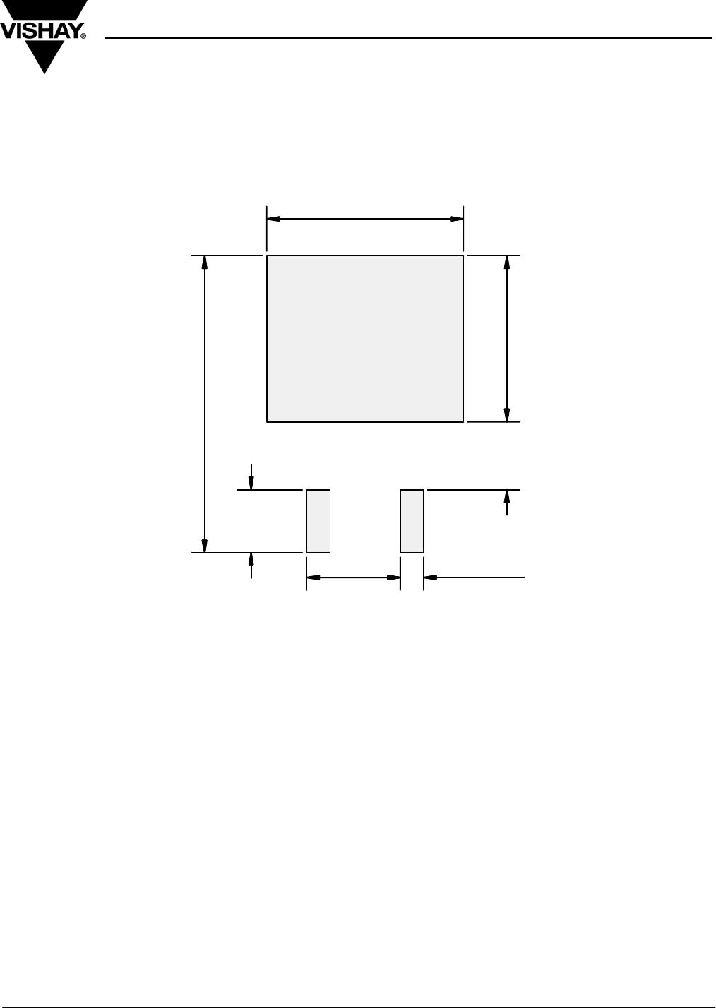
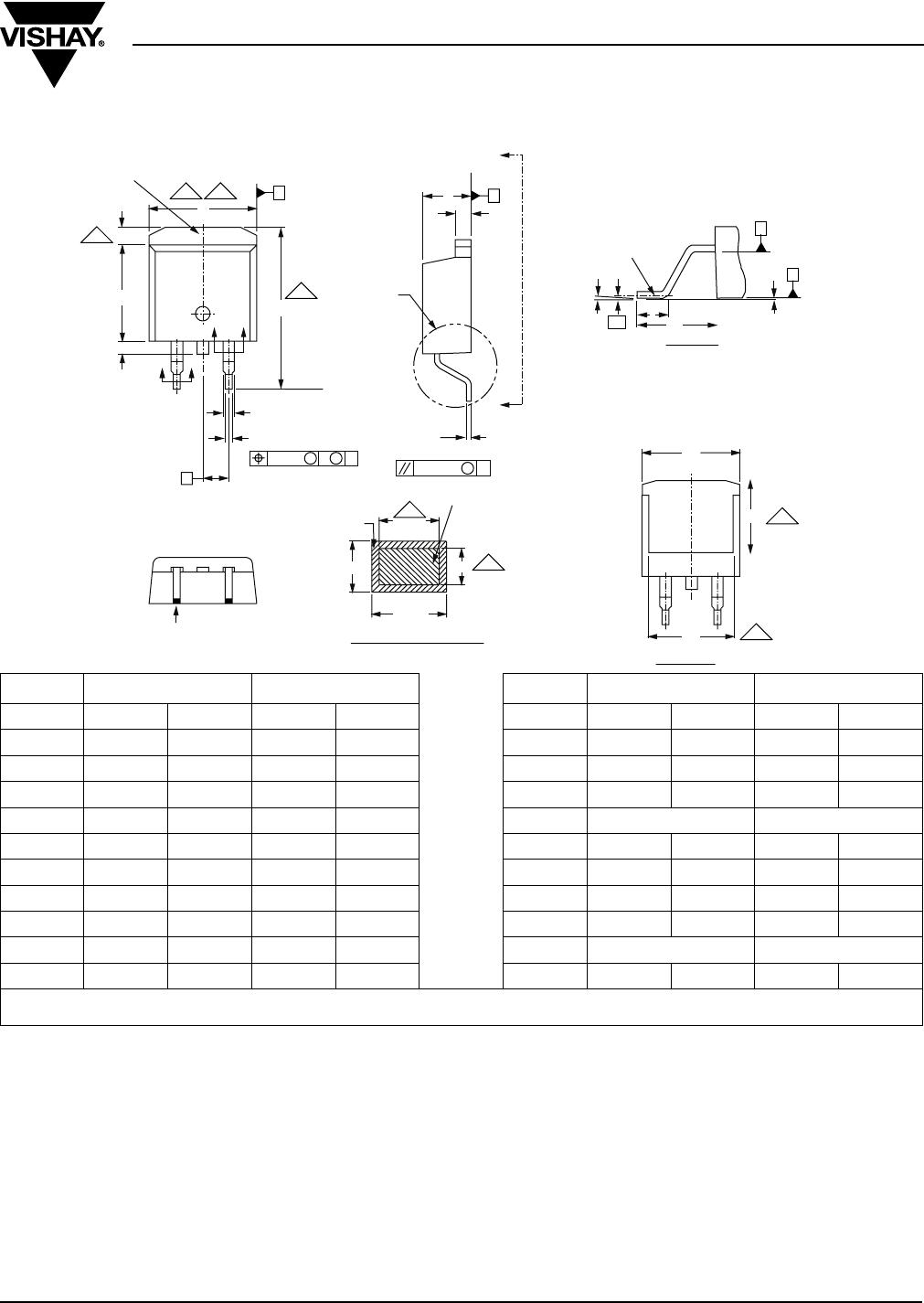
Package Information
Vishay Siliconix
TO-263AB (HIGH VOLTAGE)
Notes
1. Dimensioning and tolerancing per ASME Y14.5M-1994.
2. Dimensions are shown in millimeters (inches).
3. Dimension D and E do not include mold flash. Mold flash shall not exceed 0.127 mm (0.005") per side. These dimensions are measured at the
outmost extremes of the plastic body at datum A.
4. Thermal PAD contour optional within dimension E, L1, D1 and E1.
5. Dimension b1 and c1 apply to base metal only.
6. Datum A and B to be determined at datum plane H.
7. Outline conforms to JEDEC outline to TO-263AB.
5
4
1
3
L1
L2
D
B
B
E
H
B
A
Detail A
A
A
c
c2
A
2 x e
2 x b2
2 x b
0.010 A B
MM
± 0.004 B
M
Base
metal
Plating
b1, b3
(b, b2)
c1
(c)
Section B - B and C - C
Scale: none
Lead tip
4
34
(Datum A)
2
C
C
B
B
5
5
View A - A
E1
D1
E
4
4
B
H
Seating plane
Gauge
plane
0° to 8°
Detail “A”
Rotated 90° CW
scale 8:1
L3
A1
L4
L
MILLIMETERS INCHES MILLIMETERS INCHES
DIM. MIN. MAX. MIN. MAX. DIM. MIN. MAX. MIN. MAX.
A 4.06 4.83 0.160 0.190 D1 6.86 - 0.270 -
A1 0.00 0.25 0.000 0.010 E 9.65 10.67 0.380 0.420
b 0.51 0.99 0.020 0.039 E1 6.22 - 0.245 -
b1 0.51 0.89 0.020 0.035 e 2.54 BSC 0.100 BSC
b2 1.14 1.78 0.045 0.070 H 14.61 15.88 0.575 0.625
b3 1.14 1.73 0.045 0.068 L 1.78 2.79 0.070 0.110
c 0.38 0.74 0.015 0.029 L1 - 1.65 - 0.066
c1 0.38 0.58 0.015 0.023 L2 - 1.78 - 0.070
c2 1.14 1.65 0.045 0.065 L3 0.25 BSC 0.010 BSC
D 8.38 9.65 0.330 0.380 L4 4.78 5.28 0.188 0.208
ECN: S-82110-Rev. A, 15-Sep-08
DWG: 5970
AN826
Vishay Siliconix
Document Number: 73397
11-Apr-05
www.vishay.com
1
RECOMMENDED MINIMUM PADS FOR D
2
PAK: 3-Lead
0.635
(16.129)
Recommended Minimum Pads
Dimensions in Inches/(mm)
0.420
(10.668)
0.355
(9.017)
0.145
(3.683)
0.135
(3.429)
0.200
(5.080)
0.050
(1.257)
Return to Index

IRFBC40SPBF

Mfr. #:
Manufacturer:
Vishay / Siliconix
Description:
MOSFET N-Chan 600V 6.2 Amp
Lifecycle:
New from this manufacturer.
Delivery:
DHL FedEx Ups TNT EMS
Payment:
T/T Paypal Visa MoneyGram Western Union