6V40088CNBGI8

IDT6V40088
DUAL OUTPUT SPREAD SPECTRUM CLOCK SYNTHESIZER CLOCK SYNTHESIZER
IDT®
DUAL OUTPUT SPREAD SPECTRUM CLOCK SYNTHESIZER 4
IDT6V40088 REV E 121409
Absolute Maximum Ratings
Stresses above the ratings listed below can cause permanent damage to the IDT6V40088. These ratings, which
are standard values for IDT commercially rated parts, are stress ratings only. Functional operation of the device at
these or any other conditions above those indicated in the operational sections of the specifications is not implied.
Exposure to absolute maximum rating conditions for extended periods can affect product reliability. Electrical
parameters are guaranteed only over the recommended operating temperature range.
Recommended Operation Conditions
Parameter Condition Min. Typ. Max. Units
Supply Voltage, VDD Referenced to GND -0.5 7 V
Inputs Referenced to GND -0.5 VDD+ 0.5 V
Clock Outputs Referenced to GND -0.5 VDD+ 0.5 V
Storage Temperature -65 150 ° C
Soldering Temperature Max 10 seconds 260 ° C
Junction Temperature 125 ° C
Parameter Min. Typ. Max. Units
Ambient Operating Temperature -40 +85 ° C
Power Supply Voltage (measured in respect to GND) +2.97 +3.3 +3.63 V
Power Supply Ramp Time 4 ms
IDT6V40088
DUAL OUTPUT SPREAD SPECTRUM CLOCK SYNTHESIZER CLOCK SYNTHESIZER
IDT®
DUAL OUTPUT SPREAD SPECTRUM CLOCK SYNTHESIZER 5
IDT6V40088 REV E 121409
DC Electrical Characteristics
Unless stated otherwise, VDD = 3.3 V ±10%, Ambient Temperature -40 to +85° C
Parameter Symbol Conditions Min. Typ. Max. Units
Operating Voltage VDD 2.97 3.3 3.63 V
Operating Supply Current IDD C
L
= 15 pF, VDD = 3.63 V,
T
A
= +85°C
47 55 mA
C
L
= 5 pF, VDD = 3.63 V,
T
A
= +85°C
44 47
Input High Voltage V
IH
VDD-0.8 V
Input Low Voltage V
IL
S0:S1 0.8 V
Input Mid Voltage V
IM
S0:S1 VDD/2-0.4 VDD/2+0.4 V
Input High Voltage V
IH
ICLK VDD/2+1 V
Input Low Voltage V
IL
ICLK VDD/2-1 V
Output High Voltage V
OH
I
OH
= -12 mA VDD-0.4 V
Output Low Voltage V
OL
I
OL
= 12 mA 0.4 V
Short Circuit Current I
OS
±70 mA
Nominal Output
Impedance
Z
O
20 Ω
Internal Pull-down
Resistor
R
PD
S0, S1 200 260 kΩ
Input Capacitance C
IN
inputs 5 pF
IDT6V40088
DUAL OUTPUT SPREAD SPECTRUM CLOCK SYNTHESIZER CLOCK SYNTHESIZER
IDT®
DUAL OUTPUT SPREAD SPECTRUM CLOCK SYNTHESIZER 6
IDT6V40088 REV E 121409
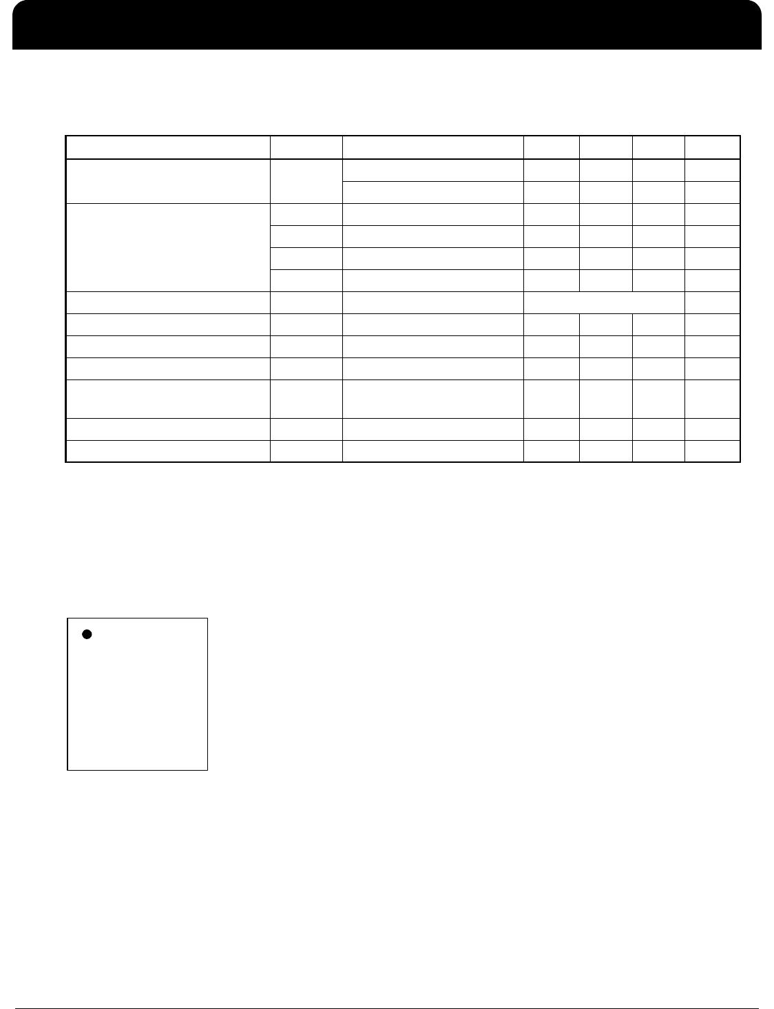
AC Electrical Characteristics
Unless stated otherwise, VDD = 3.3 V ±10%, Ambient Temperature -40 to +85° C, C
L
= 5 pF
Note 1: 27M measured with 5 pF load.
Note 2: 27M measured with 15 pF load.
Note 3: 100M measured with 5 pF load.
Note 4: 100M measured with 15 pF load.
* Spread 2% and below.
Marking Diagram
Notes:
1. ### is the lot number.
2. YYW is the last digit of the year and week that the part was assembled. “$” is the assembler mark code.
3. “8C” is the truncated part number and revision ID.
4. “G” denotes RoHS compliant package.
5. “I” denotes industrial temperature range.
6. Bottom marking: country of origin.
Parameter Symbol Conditions Min. Typ. Max. Units
Input Frequency F
IN
Fundamental Crystal 27 MHz
Input Clock 27 MHz
Output Rise/Fall Time t
RF5
20% to 80%, Note 1 1 1.5 ns
t
RF15
80% to 20%, Note 2 1.5 2 ns
t
RF5
20% to 80%, Note 3 0.75 1 ns
t
RF15
20% to 80%, Note 4 1.5 1.75 ns
Synthesis Error t
PPM
100M output 0 ppm
Duty Cycle t
DC
45 50 55 %
Modulation Frequency f
MOD
100M 32 kHz
Modulation Type Slew Rate 100M output, triangular* 0.125 %/µs
Power-up Time PLL lock time from
power-up
5ms
Cycle-to-cycle Jitter 125 200 ps
Long-term Jitter (10,000 cycles) S0=S1=0, 100M, 27M 200 300 ps
###
YWW$
8CGI

6V40088CNBGI8

Mfr. #:
Manufacturer:
IDT
Description:
Clock Generators & Support Products LCD Graphics Clock for AMD
Lifecycle:
New from this manufacturer.
Delivery:
DHL FedEx Ups TNT EMS
Payment:
T/T Paypal Visa MoneyGram Western Union

Products related to this Datasheet