4
NO-DESIGN SWITCHER
DEMO MANUAL DC237/DC238
DC237 vs DC238 (Temperature vs Package Size)
The DC237 and DC238 demonstration boards are
intended for evaluation of the LT1506 switching regulator
in the SO-8 and 7-pin DD packages respectively. The 7-pin
DD package used in DC238 has no SYNC pin, but a version
(LT1506CR-SYNC) replaces the SHDN function at Pin 2
with the SYNC function. The primary reason for choosing
the SO-8 over the DD package is board space. The DC238
(DD package) occupies an active board area of approxi-
mately 0.75 square inches. Optimizing the DC237 board,
using a Sumida coil and removing the layout options, a
total active area of 0.4 square inches is possible. The DD
package is more suitable for higher power or higher am-
bient temperature applications. Although both boards will
supply 4A of output current, DC237 must be thermally
derated to 3A continuous at 22°C ambient to prevent ex-
cessive die temperatures. DC238 can run at 60°C ambient
at 4A output current. However, the SO-8 package can be
used for dynamic loads up to the full rated switch current.
LT1506 Operation
The LT1506 data sheet gives a complete description of the
part, operation and applications information. The data
sheet should be read in conjunction with this demo manual.
Hook-Up
Solid turret terminals are provided for easy connection to
supplies and test equipment. Connect a 0V to 15V, 4.5A
power supply across the V
IN
and GND terminals and the
load across the V
OUT
and GND terminals. When measuring
load/line regulation, remember to Kelvin connect to the
turrets. Also, when measuring output ripple voltage with
an oscilloscope probe, the wire from the probe to the
ground clip will act as an antenna, picking up excessive
noise. For improved results, the test hook should be
removed from the tip of the probe. The tip should be
touched against the output turret, with the bare ground
shield pressed against the ground turret. This reduces the
noise seen on the waveform.
Shutdown
For normal operation, the SHDN pin can be left floating.
SHDN has two output-disable modes: lockout and
OPERATIO
U
shutdown. When the pin is taken below the lockout
threshold, switching is disabled. This is typically used for
input undervoltage lockout. Grounding the SHDN pin
places the LT1506 in shutdown mode. This reduces total
board supply current to 20µA.
Synchronization
Synchronization is Available on DC237 Only (SYNC
is an Optional Replacement for SHDN on the DD
Package).For normal demo board operation, the SYNC pin
can be left floating. If unused in the application, it is
advisable to tie this pin to ground. To synchronize switch-
ing to an external clock, apply a logic-level signal to the
SYNC pin. The amplitude must be from a logical low to
greater than 2.2V, with a duty cycle from 10% to 90%. The
synchronization frequency must be greater than the free-
running oscillator frequency and less than 1MHz. Addi-
tional circuitry may be required to prevent subharmonic
oscillation. Refer to the LT1506 data sheet for more
details.
COMPONENTS
Inductor L1
The inductor is a Coilcraft DO3316P-682, a 6.8µH
unshielded ferrite unit. It was selected for its low cost,
small size and 4.6A I
SAT
rating. The equivalent Coiltronics
UP2-6R8 unit can be substituted. If board space is at a
premium and higher ripple current is acceptable, solder
pads are available for the Sumida CD43-1R8 inductor.
This 1.8µH unit has a 2.9A I
SAT
rating. Ripple at 5V
IN
is
±1.1A. This gives a maximum output current of
(4.5A – 1.1A) = 3.4A.
Input/Output Capacitors C3, C5, C6 and C7
The input capacitor C3 is a Tokin ceramic capacitor. It was
selected for its small size, high voltage rating and low ESR
(effective series resistance). The input ripple current for a
buck converter is high, typically I
OUT
/2. Tantalum capaci-
tors become resistive at higher frequencies, requiring
careful ripple-rating selection to prevent excessive heat-
ing. Ceramic capacitors’ ESL (effective series inductance)
tends to dominate their ESR, making them less suscep-
tible to ripple-induced heating.
5
DEMO MANUAL DC237/DC238
NO-DESIGN SWITCHER
OPERATIO
U
The output capacitor C5 is an AVX tantalum capacitor. A
ceramic is not recommended as the main output capacitor
since loop stability relies on a resistive characteristic at
higher frequencies to form a zero. The AVX TPS series was
specifically designed for switch-mode power supplies to
have very low ESR. At switching frequencies, ripple volt-
age is more a function of ESR than of absolute capacitance
value. If lower output ripple voltage is required, use the
optional capacitor C7 to reduce ESR rather than increasing
the capacitance of C5. For very low ripple, an additional LC
filter in the output may be a less expensive solution. The
output contains very narrow voltage spikes because of the
parasitic inductance of C5. A small ceramic capacitor, C6,
removes these spikes on the demo board. In application,
trace inductance and local bypass capacitors will perform
this function, negating the need for C6.
Catch Diode D1
Use diodes designed for switching applications, with
adequate current rating and fast turn-on times, such as
Schottky or ultrafast diodes. In selecting a diode, the basic
parameters of interest are forward voltage, maximum
reverse voltage, average operating current and peak cur-
rent. Lower forward voltage yields higher circuit efficiency
and lowers power dissipation in the diode. The MBRD835L
has a maximum forward drop of 0.4V at 3A. The reverse
voltage rating must be greater than the input voltage.
Average diode current is always less than output current,
but under a shorted output condition, diode current can
equal switch current limit. If the application must with-
stand this condition, the diode must be rated for maximum
switch current.
Compensation: C1, C2 and R1
A detailed discussion of frequency compensation can be
found in the LT1506 data sheet. C1, a 1500pF capacitor
from V
C
to ground, gives a stable loop response over a
wide range of input and output conditions. Options R1 and
C2 are included for optimization of the dynamic response
to a specific application.
Boost Voltage: D2, D3 and C4
A boost voltage of at least 2.8V is required throughout
the on-time of the switch to guarantee that it remains
saturated. At output currents greater than 3A and
higher ambient temperatures, diode D2 must be moved
to position D3 to prevent boost from falling below this
minimum. For output voltages above 3.3V, diode D2
provides sufficient boost voltage to C4.
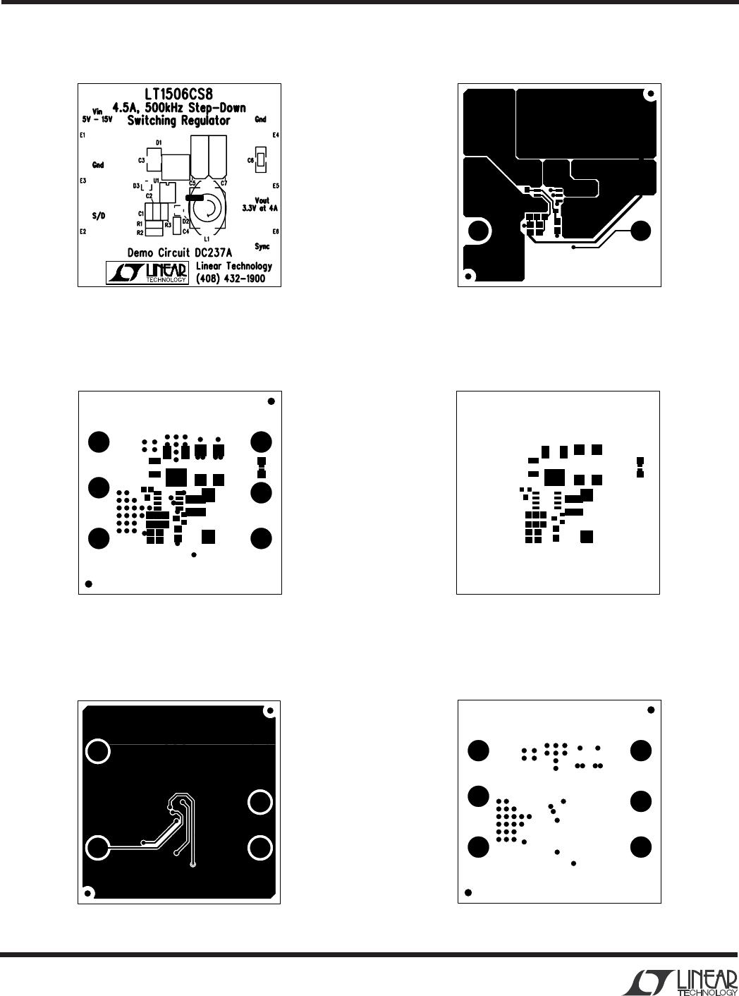
PCB LAYOUT
In many cases, the layout of the demonstration board
may be dropped directly into the application with mini-
mal changes. If not, there are several precautions that
must be taken when laying out high frequency con-
verter circuits. The high frequency switching path runs
from ground, through C3, to the V
IN
pin of the LT1506,
out of the SW pin, through D1 and back to ground. This
loop acts as an antenna and will radiate noise if not kept
as short as possible. Also, at higher switching currents,
the associated trace inductance can cause excessive
voltage spikes across the switch. The use of a ground
plane will reduce many noise problems. The ground pin
of the LT1506 contains some high frequency signal
currents, but more importantly, it is the 0V reference for
the output voltage. Connect the ground pin directly to
the ground plane. The FB and V
C
components should be
kept away from the power components as much as
possible. The ground for these components should be
separated from power grounds. Run a Kelvin sense to
V
OUT
as required but keep the divider network close to
the LT1506 to prevent noise pickup on the FB node.
Noise pickup on the V
C
pin appears as various prob-
lems, including poor load regulation, subharmonic
oscillation and instability. Thermal management must
also be considered. The SO-8 package has a fused
ground pin. Soldering this pin to a large copper area will
significantly reduce its thermal resistance. Solder-filled
feedthroughs close to the ground pin provide a good
thermal path to the ground plane. For the DD package,
the grounded tab should be treated in the same manner.
For more information or advice, contact the LTC Appli-
cations department.
6
NO-DESIGN SWITCHER
DEMO MANUAL DC237/DC238
PCB LAYOUT A D FIL
UW
(DC237)
Component Side Silkscreen
Component Side
Solder Side Solder Side Solder Mask
Component Side Paste MaskComponent Side Solder Mask

DC237A

Mfr. #:
Manufacturer:
Analog Devices Inc.
Description:
Power Management IC Development Tools LT1506CS8 - 4.5A SWITCH, 500KHz STEP DOW
Lifecycle:
New from this manufacturer.
Delivery:
DHL FedEx Ups TNT EMS
Payment:
T/T Paypal Visa MoneyGram Western Union

Products related to this Datasheet