©2005 Fairchild Semiconductor Corporation www.fairchildsemi.com
4NXXM, H11AXM Rev. 1.0.2 2
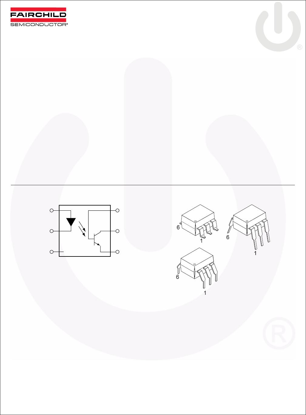
4NXXM, H11AXM — General Purpose 6-Pin Phototransistor Optocouplers
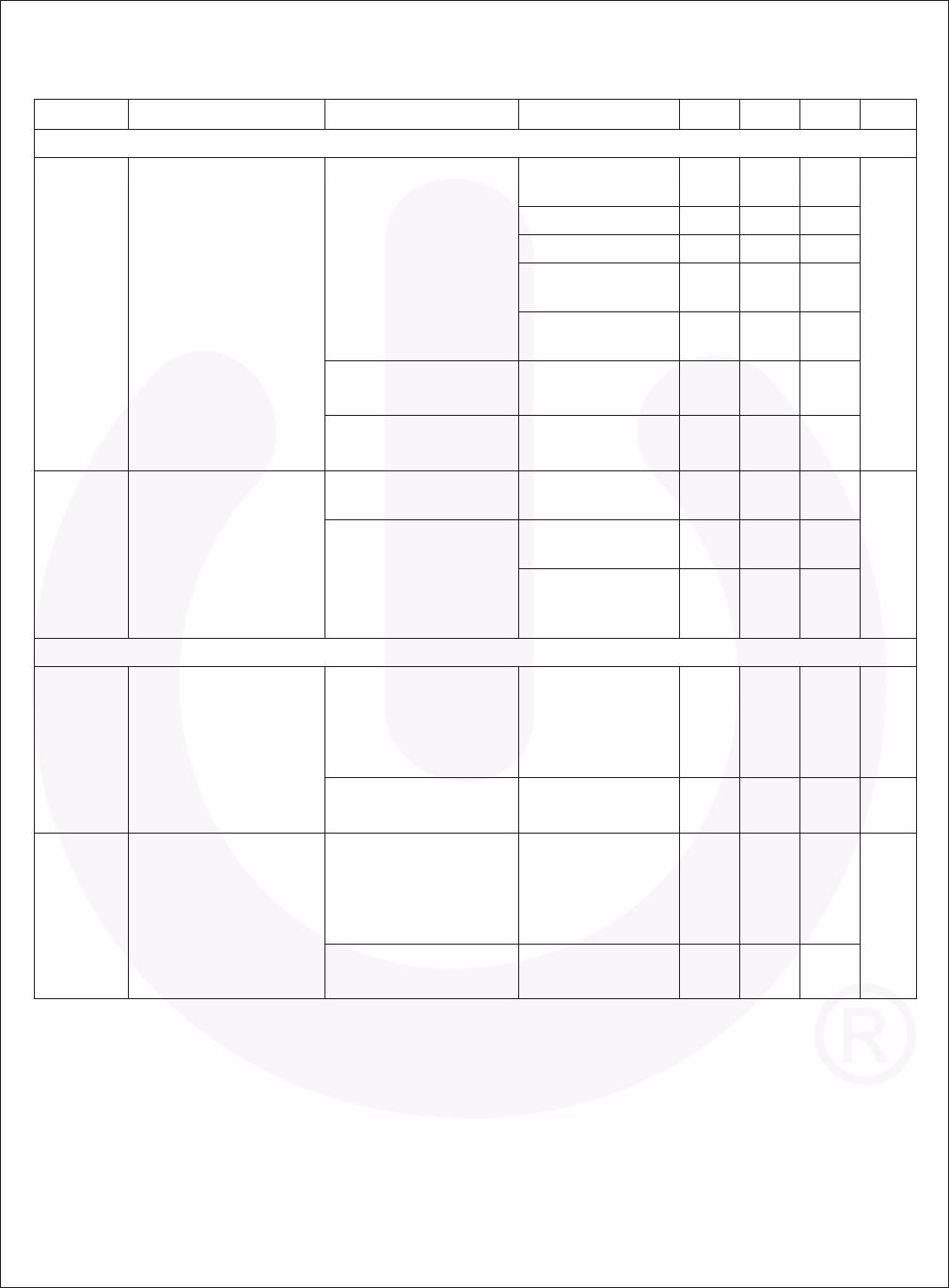
Absolute Maximum Ratings
(T
A
= 25°C unless otherwise specified)
Stresses exceeding the absolute maximum ratings may damage the device. The device may not function or be
operable above the recommended operating conditions and stressing the parts to these levels is not recommended.
In addition, extended exposure to stresses above the recommended operating conditions may affect device reliability.
The absolute maximum ratings are stress ratings only.
Electrical Characteristics
(T
A
= 25°C unless otherwise specified)
Individual Component Characteristics
Isolation Characteristics
*Typical values at T
A
= 25°C
Symbol Parameter Value Units
TOTAL DEVICE
T
STG
Storage Temperature -40 to +150 °C
T
OPR
Operating Temperature -40 to +100 °C
T
SOL
Wave solder temperature (see page 8 for reflow solder profile) 260 for 10 sec °C
P
D
Total Device Power Dissipation @ T
A
= 25°C
Derate above 25°C
250 mW
2.94
EMITTER
I
F
DC/Average Forward Input Current 60 mA
V
R
Reverse Input Voltage 6 V
I
F
(pk) Forward Current – Peak (300µs, 2% Duty Cycle) 3 A
P
D
LED Power Dissipation @ T
A
= 25°C
Derate above 25°C
120 mW
1.41 mW/°C
DETECTOR
V
CEO
Collector-Emitter Voltage 30 V
V
CBO
Collector-Base Voltage 70 V
V
ECO
Emitter-Collector Voltage 7 V
P
D
Detector Power Dissipation @ T
A
= 25°C
Derate above 25°C
150 mW
1.76 mW/°C
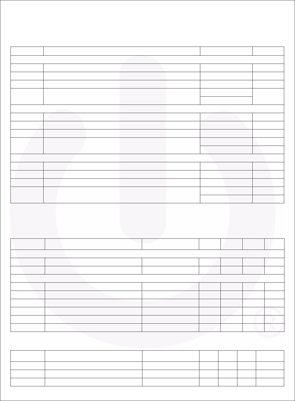
Symbol Parameter Test Conditions Min. Typ.* Max. Unit
EMITTER
V
F
Input Forward Voltage I
F
= 10mA 1.18 1.50 V
I
R
Reverse Leakage Current V
R
= 6.0V 0.001 10 µA
DETECTOR
BV
CEO
Collector-Emitter Breakdown Voltage I
C
= 1.0mA, I
F
= 0 30 100 V
BV
CBO
Collector-Base Breakdown Voltage I
C
= 100µA, I
F
= 0 70 120 V
BV
ECO
Emitter-Collector Breakdown Voltage I
E
= 100µA, I
F
= 0 7 10 V
I
CEO
Collector-Emitter Dark Current V
CE
= 10V, I
F
= 0 1 50 nA
I
CBO
Collector-Base Dark Current V
CB
= 10V 20 nA
C
CE
Capacitance V
CE
= 0V, f = 1 MHz 8 pF
Symbol Characteristic Test Conditions Min. Typ.* Max. Units
V
ISO
Input-Output Isolation Voltage f = 60Hz, t = 1 sec 7500 Vac(pk)
R
ISO
Isolation Resistance V
I-O
= 500 VDC 10
11
Ω
C
ISO
Isolation Capacitance V
I-O
= &, f = 1MHz 0.2 2 pF