LTC2636
18
2636fc
For more information www.linear.com/LTC2636
OPERATION
2636 F02
C3
COMMAND ADDRESS
MSB
MSB
MSB
LSB
LSB
LSB
DATA (12 BITS + 4 DON'T-CARE BITS)
C2 C1 C0 A3 A2 A1 A0 D11 D10 D9 D8 D7 D6 D5 D4 D3 D2 D1 D0 X X X X
C3
COMMAND ADDRESS DATA (10 BITS + 6 DON'T-CARE BITS)
C2 C1 C0 A3 A2 A1 A0 D9 D8 D7 D6 D5 D4 D3 D2 D1 D0 X X X X X X
C3
COMMAND
INPUT WORD (LTC2636-12)
INPUT WORD (LTC2636-10)
INPUT WORD (LTC2636-8)
ADDRESS DATA (8 BITS + 8 DON'T-CARE BITS)
C2 C1 C0 A3 A2 A1 A0 D7 D6 D5 D4 D3 D2 D1 D0 X X X X X X X X
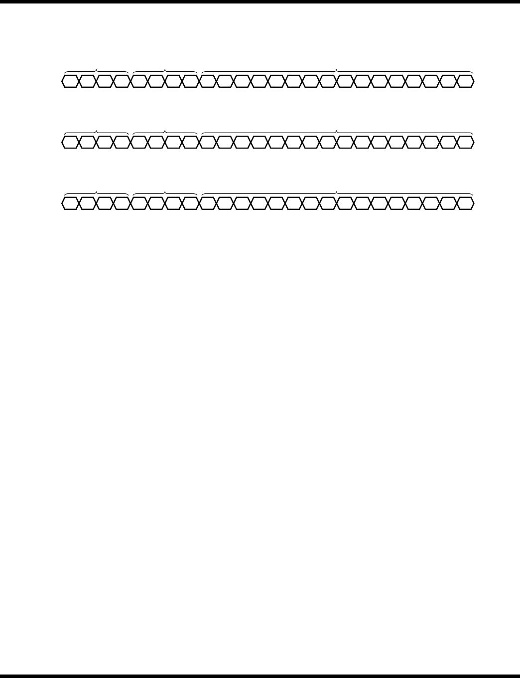
Figure 2. Command and Data Input Format
Serial Interface
The CS/LD input is level triggered. When this input is
taken low, it acts as a chip-select signal, enabling the SDI
and SCK buffers and the input shift register. Data (SDI
input) is transferred into the LTC2636 on the next 24 ris-
ing SCK edges. The 4-bit command, C3-C0, is loaded first;
then the 4-bit DAC address, A3-A0; and finally the 16-bit
data word. The data word comprises the 12-, 10- or 8-bit
input code, ordered MSB-to-LSB, followed by 4, 6 or 8
don’t-care bits (LTC2636-12, -10 and -8 respectively; see
Figure 2). Data can only be transferred to the device when
the CS/LD signal is low, beginning on the first rising edge
of SCK. SCK may be high or low at the falling edge of
CS/LD. The rising edge of CS/LD ends the data transfer
and causes the device to execute the command specified
in the 24-bit input sequence. The complete sequence is
shown in Figure 3a.
The command (C3-C0) and address (A3-A0) assignments
are shown in Tables 1 and 2. The first four commands in
Table 1 consist of write and update operations. A Write
operation loads a 16-bit data word from the 24-bit shift
register into the input register of the selected DAC, n. An
Update operation copies the data word from the input
register to the DAC register. Once copied into the DAC
register, the data word becomes the active 12-, 10-, or
8-bit input code, and is converted to an analog voltage at
the DAC output. Write to and Update combines the first
two commands. The Update operation also powers up the
DAC if it had been in power-down mode. The data path
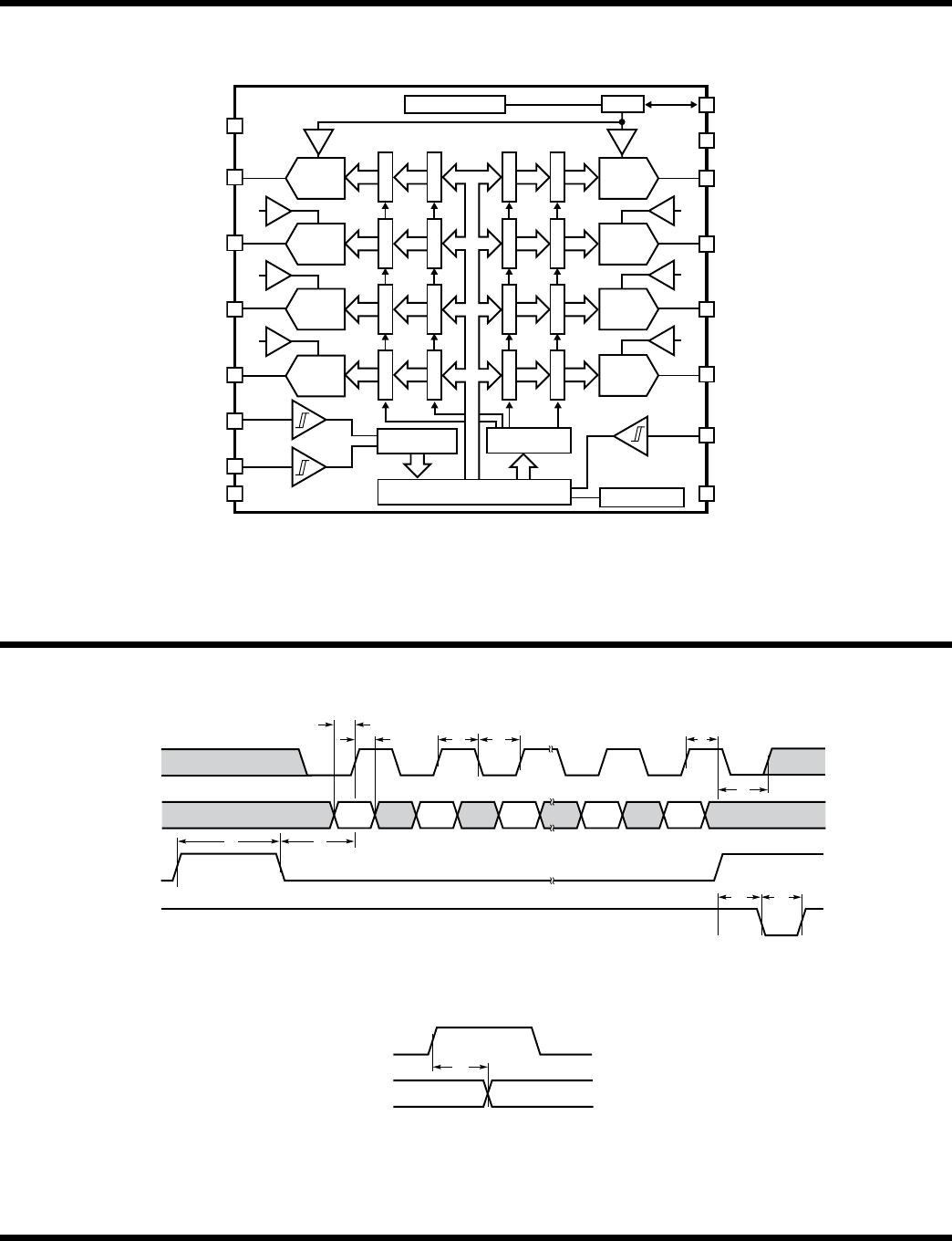
and registers are shown in the Block Diagram.
While the minimum input sequence is 24 bits, it may
optionally be extended to 32 bits to accommodate micro-
processors that have a minimum word width of 16 bits
(2 bytes). To use the
32-bit width, 8 don’t-care bits must
be transferred to the device first, followed by the 24-bit
sequence described. Figure 3b shows the 32-bit sequence.
The 16-bit data word is ignored for all commands that do
not include a Write operation.
Reference Modes
For applications where an accurate external reference is
either not available, or not desirable due to limited space,
the LTC2636 has a user-selectable, integrated reference.
The integrated reference voltage is internally amplified
by 2x to provide the full-scale DAC output voltage range.
The LTC2636-LMI/-LMX/-LZ provides a full-scale DAC
output of 2.5V. The LTC2636-HMI/-HMX/-HZ provides a
full-scale DAC output of 4.096V. The internal reference
can be useful in applications where the supply voltage is
poorly regulated. Internal Reference mode can be selected
by using command 0110b, and is the power-on default
for LTC2636-HZ/-LZ, as well as for LTC2636-HMI/-LMI.
The 10ppm/°C, 1.25V (LTC2636-LMI/-LMX/-LZ) or 2.048V
(LTC2636-HMI/-HMX/-HZ) internal reference is available