1.5KA6.8 thru 1.5KA47A
www.vishay.com
Vishay General Semiconductor
Revision: 09-Feb-11
2
Document Number: 88300
For technical questions within your region: DiodesAmericas@vishay.com
, DiodesAsia@vishay.com, DiodesEurope@vishay.com
THIS DOCUMENT IS SUBJECT TO CHANGE WITHOUT NOTICE. THE PRODUCTS DESCRIBED HEREIN AND THIS DOCUMENT
ARE SUBJECT TO SPECIFIC DISCLAIMERS, SET FORTH AT www.vishay.com/doc?91000
Notes
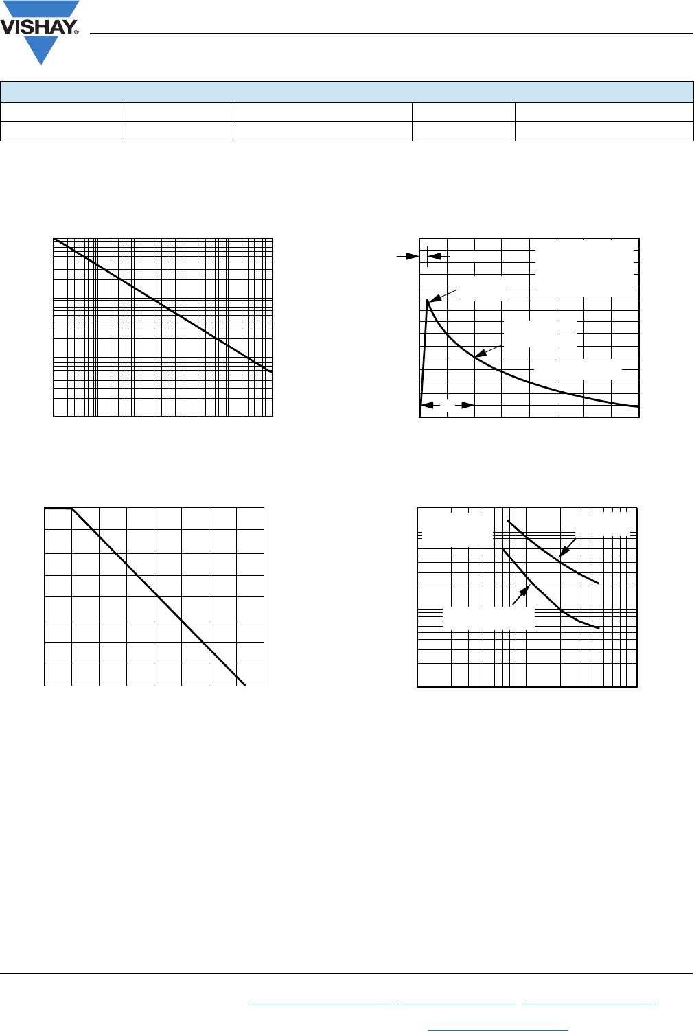
(1)
V
BR
measured after I
T
applied for 300 μs = square wave pulse or equivalent
(2)
Surge current waveform per fig. 3 and derate per fig. 2
(3)
All terms and symbols are consistent with ANSI/IEEE C62.35
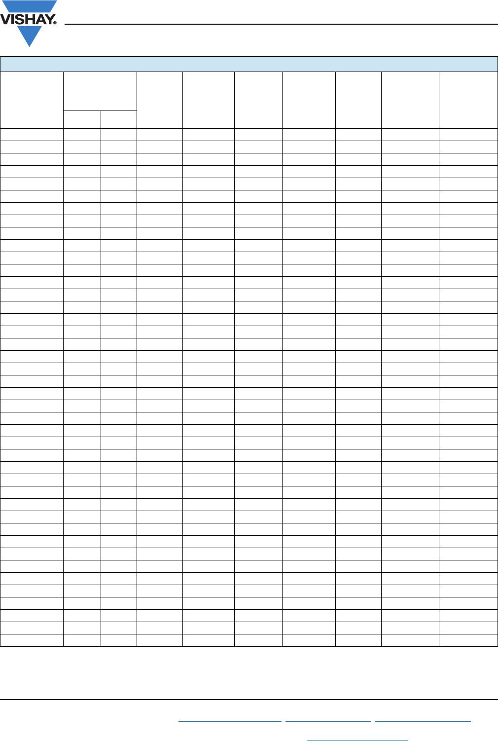
ELECTRICAL CHARACTERISTICS (T
A
= 25 °C unless otherwise noted)
DEVICE TYPE
BREAKDOWN
VOLTAGE
V
BR
(1)
AT I
T
(V)
TEST
CURRENT
I
T
(mA)
STAND-OFF
VOLTAGE
V
WM
(V)
MAXIMUM
REVERSE
LEAKAGE
AT V
WM
I
D
(μA)
T
J
= 150 °C
MAXIMUM
REVERSE
LEAKAGE
AT V
WM
I
D
(μA)
PEAK
PULSE
CURRENT
I
PPM
(2)
(A)
MAXIMUM
CLAMPING
VOLTAGE
AT I
PPM
V
C
(V)
MAXIMUM
TEMP.
COEFFICIENT
OF V
BR
(%/°C)
MIN. MAX.
1.5KA6.8 6.12 7.48 10 5.50 1000 10 000 139 10.8 0.057
1.5KA6.8A 6.45 7.14 10 5.80 1000 10 000 143 10.5 0.057
1.5KA7.5 6.75 8.25 10 6.05 500 5000 128 11.7 0.061
1.5KA7.5A 7.13 7.88 10 6.40 500 5000 133 11.3 0.061
1.5KA8.2 7.38 9.02 10 6.63 200 2000 120 12.5 0.065
1.5KA8.2A 7.79 8.61 10 7.02 200 2000 124 12.1 0.065
1.5KA9.1 8.19 10.0 1.0 7.37 50 500 109 13.8 0.068
1.5KA9.1A 8.65 9.55 1.0 7.78 50 500 112 13.4 0.068
1.5KA10 9.00 11.0 1.0 8.10 20 200 100 15.0 0.073
1.5KA10A 9.50 10.5 1.0 8.55 20 200 103 14.5 0.073
1.5KA11 9.90 12.1 1.0 8.92 5.0 50 92.6 16.2 0.075
1.5KA11A 10.5 11.6 1.0 9.40 5.0 50 96.2 15.6 0.076
1.5KA12 10.8 13.2 1.0 9.72 2.0 10 86.7 17.3 0.076
1.5KA12A 11.4 12.6 1.0 10.2 2.0 10 89.8 16.7 0.078
1.5KA13 11.7 14.3 1.0 10.5 2.0 10 78.9 19.0 0.081
1.5KA13A 12.4 13.7 1.0 11.1 2.0 10 82.4 18.2 0.081
1.5KA15 13.5 16.3 1.0 12.1 1.0 10 68.2 22.0 0.084
1.5KA15A 14.3 15.8 1.0 12.8 1.0 10 70.8 21.2 0.084
1.5KA16 14.4 17.6 1.0 12.9 1.0 10 63.8 23.5 0.086
1.5KA16A 15.2 16.8 1.0 13.6 1.0 10 66.7 22.5 0.086
1.5KA18 16.2 19.8 1.0 14.5 1.0 10 56.6 26.5 0.088
1.5KA18A 17.1 18.9 1.0 15.3 1.0 10 59.5 25.2 0.088
1.5KA20 18.0 22.0 1.0 16.2 1.0 10 51.5 29.1 0.090
1.5KA20A 19.0 21.0 1.0 17.1 1.0 10 54.2 27.7 0.090
1.5KA22 19.8 24.2 1.0 17.8 1.0 10 47.0 31.9 0.092
1.5KA22A 20.9 23.1 1.0 18.8 1.0 10 49.0 30.6 0.092
1.5KA24 21.6 26.4 1.0 19.4 1.0 10 43.2 34.7 0.094
1.5KA24A 22.8 25.2 1.0 20.5 1.0 10 45.2 33.2 0.094
1.5KA27 24.3 29.7 1.0 21.8 1.0 10 38.4 39.1 0.096
1.5KA27A 25.7 28.4 1.0 23.1 1.0 10 40.0 37.5 0.096
1.5KA30 27.0 33.0 1.0 24.3 1.0 10 34.5 43.5 0.097
1.5KA30A 28.5 31.5 1.0 25.6 1.0 10 36.2 41.4 0.097
1.5KA33 29.7 36.3 1.0 26.8 1.0 10 31.4 47.7 0.098
1.5KA33A 31.4 34.7 1.0 28.2 1.0 10 32.8 45.7 0.098
1.5KA36 32.4 39.6 1.0 29.1 1.0 10 28.8 52.0 0.099
1.5KA36A 34.2 37.8 1.0 30.8 1.0 10 30.1 49.9 0.099
1.5KA39 35.1 42.9 1.0 31.6 1.0 10 26.6 56.4 0.100
1.5KA39A 37.1 41.0 1.0 33.3 1.0 10 27.8 53.9 0.100
1.5KA43 38.7 47.3 1.0 34.8 1.0 20 24.2 61.9 0.101
1.5KA43A 40.9 45.2 1.0 36.8 1.0 20 25.3 59.3 0.101
1.5KA47 42.3 51.7 1.0 38.1 1.0 20 22.1 67.8 0.101
1.5KA47A 44.7 49.4 1.0 40.2 1.0 20 23.1 64.8 0.101