NB2309AI1HDR2G

NB2309A
www.onsemi.com
4
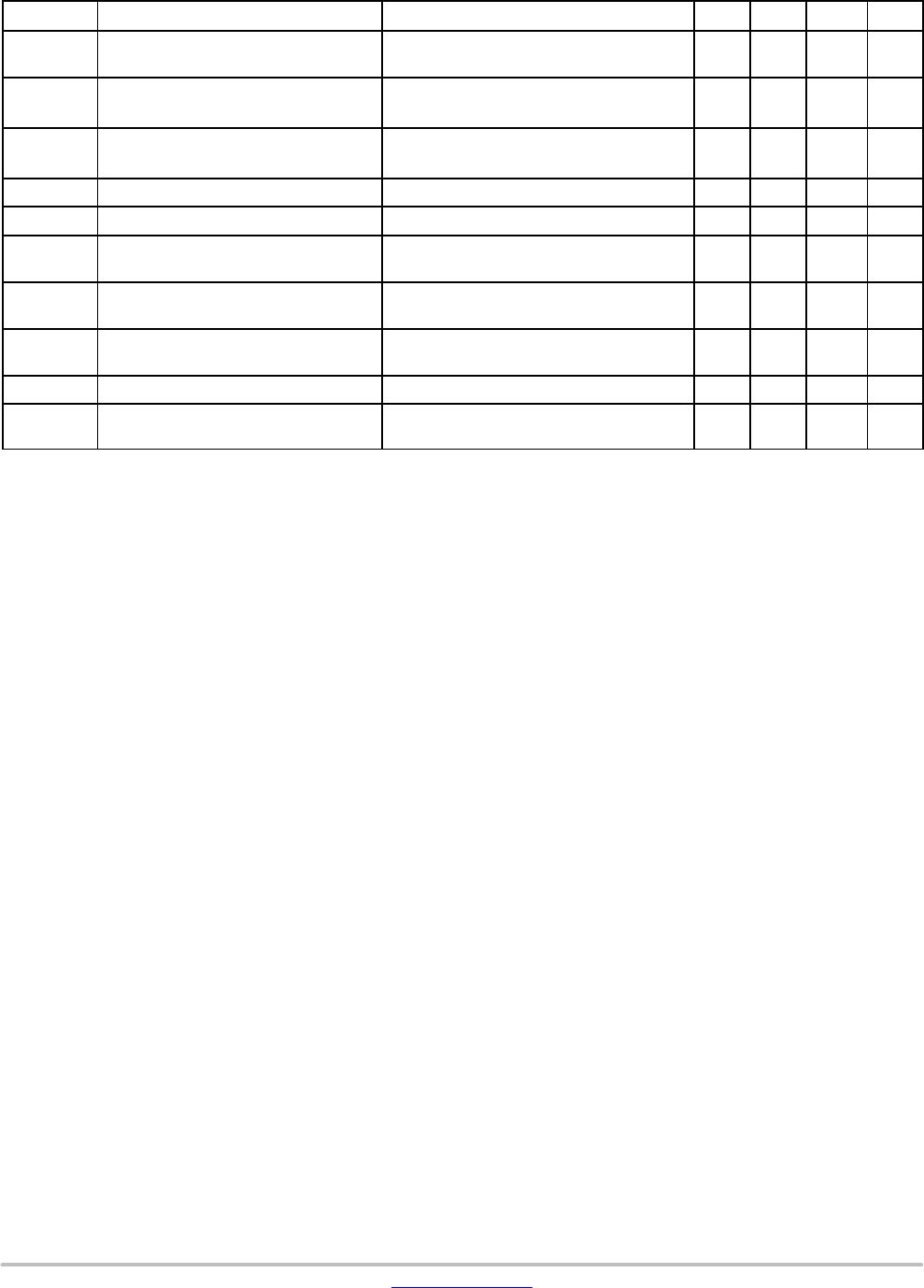
Table 3. MAXIMUM RATINGS
Parameter Min Max Unit
Supply Voltage to Ground Potential −0.5 +7.0 V
DC Input Voltage (Except REF) −0.5 V
DD
+ 0.5 V
DC Input Voltage (REF) −0.5 7 V
Storage Temperature −65 +150 °C
Maximum Soldering Temperature (10 sec) 260 °C
Junction Temperature 150 °C
Static Discharge Voltage (per MIL−STD−883, Method 3015) >2000 V
Stresses exceeding those listed in the Maximum Ratings table may damage the device. If any of these limits are exceeded, device functionality
should not be assumed, damage may occur and reliability may be affected.
Table 4. RECOMMENDED OPERATING CONDITIONS
Parameter Description Min Max Unit
V
DD
Supply Voltage 3.0 3.6 V
T
A
Operating Temperature (Ambient Temperature) Industrial
Commercial
−40
0
85
70
°C
C
L
Load Capacitance, below 100 MHz 30 pF
C
L
Load Capacitance, from 100 MHz to 133 MHz 10 pF
C
IN
Input Capacitance 7 pF
Functional operation above the stresses listed in the Recommended Operating Ranges is not implied. Extended exposure to stresses beyond
the Recommended Operating Ranges limits may affect device reliability.
Table 5. ELECTRICAL CHARACTERISTICS V
CC
= 3.0 V to 3.6 V, GND = 0 V, T
A
= −40°C to +85°C
Parameter
Description Test Conditions Min Max Unit
V
IL
Input LOW Voltage (Note 5) 0.8 V
V
IH
Input HIGH Voltage (Note 5) 2.0 V
I
IL
Input LOW Current V
IN
= 0 V 50.0
A
I
IH
Input HIGH Current V
IN
= V
DD
100.0
A
V
OL
Output LOW Voltage I
OL
= 8 mA (−1)
I
OL
= 12 mA (−1H)
0.4 V
V
OH
Output HIGH Voltage I
OH
= −8 mA (−1)
I
OH
= −12 mA (−1H)
2.4 V
I
DD
Supply Current (Commercial Temp) Unloaded outputs at 66.67 MHz,
Select inputs at V
DD
34 mA
I
DD
Supply Current (Industrial Temp) Unloaded outputs at 100 MHz
66.67 MHz
33 MHz
Select inputs at V
DD
or GND, at Room
Temp
50
34
19
mA
Product parametric performance is indicated in the Electrical Characteristics for the listed test conditions, unless otherwise noted. Product
performance may not be indicated by the Electrical Characteristics if operated under different conditions.
5. REF input has a threshold voltage of V
DD
/2.
NB2309A
www.onsemi.com
5
Table 6. SWITCHING CHARACTERISTICS V
CC
= 3.0 V to 3.6 V, GND = 0 V, T
A
= −40°C to +85°C (Note 6)
Parameter
Description Test Conditions Min Typ Max Unit
1/t
1
Output Frequency 30 pF load
10 pF load
15
15
100
133
MHz
1/t
1
Duty Cycle = (t
2
/ t
1
) * 100 (−1, −1H)
(−1H)
Measured at 1.4 V, F
OUT
= 66.67 MHz
< 50 MHz
40
45
50
50
60
55
%
t
3
Output Rise Time (−1)
(−1H)
Measured between 0.8 V and 2.0 V 2.5
1.5
ns
t
4
Output Fall Time Measured between 2.0 V and 0.8 V 1.5 ns
t
5
Output−to−Output Skew All outputs equally loaded 250 ps
t
6
Delay, REF Rising Edge to CLKOUT
Rising Edge
Measured at V
DD
/2 0 ±350 ps
t
7
Device−to−Device Skew Measured at V
DD
/2 on the CLKOUT pins of
the device
0 700 ps
t
8
Output Slew Rate Measured between 0.8 V and 2.0 V using
Test Circuit #2
1 V/ns
t
J
Cycle−to−Cycle Jitter Measured at 66.67 MHz, loaded outputs 200 ps
t
LOCK
PLL Lock Time Stable power supply, valid clock presented
on REF pin
1.0 ms
6. All parameters specified with loaded outputs in PLL−Mode.
NB2309A
www.onsemi.com
6
Zero Delay and Skew Control
All outputs should be uniformly loaded to achieve Zero
Delay between input and output. Since the CLKOUT pin is
the internal feedback to the PLL, its relative loading can
adjust the input−output delay.
For applications requiring zero input−output delay, all
outputs, including CLKOUT, must be equally loaded. Even
if CLKOUT is not used, it must have a capacitive load equal
to that on other outputs, for obtaining zero−input−output
delay.
SWITCHING WAVEFORMS
Figure 3. Duty Cycle Timing
1.4 V 1.4 V 1.4 V
t
1
t
2
Figure 4. All Outputs Rise/Fall Time
t
3
OUTPUT
2.0 V
0.8 V
t
4
2.0 V
0.8 V
3.3 V
0 V
1.4 V
1.4 V
t
5
Figure 5. Output − Output Skew
OUTPUT
OUTPUT
t
6
INPUT
OUTPUT
Figure 6. Input − Output Propagation Delay
V
DD
2
V
DD
2
Figure 7. Device − Device Skew
t
7
CLKOUT, Device 1
V
DD
2
V
DD
2
CLKOUT, Device 2
TEST CIRCUITS
V
DD
V
DD
C
LOAD
GND GND
OUTPUTS
Figure 8. Test Circuit #1
10 pF
0.1 F
0.1 F
V
DD
V
DD
GND GND
OUTPUTS
0.1 F
0.1 F
1 k
1 k
Figure 9. Test Circuit #2
For parameter t
8
(output slew rate) on −1H devices
V
DD
CLKOUT

NB2309AI1HDR2G

Mfr. #:
Manufacturer:
ON Semiconductor
Description:
Phase Locked Loops - PLL 3.3V Nine Output Zero Delay Buffer
Lifecycle:
New from this manufacturer.
Delivery:
DHL FedEx Ups TNT EMS
Payment:
T/T Paypal Visa MoneyGram Western Union