BLM21AG601SN1D

Spec. No. JENF243A-0005X-01 P.7/10
MURATA MFG.CO., LTD.
Reference
Only
9. Caution
9-1. Surge current
Excessive surge current (pulse current or rush current) than specified rated current applied to the product may cause a
critical failure, such as an open circuit, burnout caused by excessive temperature rise.
Please contact us in advance in case of applying the surge current.
9-2. Limitation of Applications
Please contact us before using our products for the applications listed below which require especially high
reliability for the prevention of defects which might directly cause damage to the third party's life, body or
property.
(1)Aircraft equipment (6)Disaster prevention / crime prevention equipment
(2)Aerospace equipment (7)Traffic signal equipment
(3)Undersea equipment (8)Transportation equipment (vehicles,trains,ships,etc.)
(4)Power plant control equipment (9)Applications of similar complexity and /or reliability requirements
(5)Medical equipment to the applications listed in the above
10. Notice
This product is designed for solder mounting.
Please consult us in advance for applying other mounting method such as conductive adhesive.
10-1. Land pattern designing
Standard land dimensions
< BLM21 series(except BLM21PG/BLM21SN type) >
(in mm)
< For BLM21PG/BLM21SN type >
Type
Rated
Current
(A)
Land pad thickness
and dimension a
18µm 35µm 70µm
BLM21PG
1.5 1.0 1.0 1.0
2 1.2 1.0 1.0
34
2.4 1.2 1.0
6 6.4 3.3 1.65
BLM21SN
68.5
- 6.8 3.4
(in mm)
*The excessive heat by land pads may cause deterioration
at joint of products with substrate.
10-2. Soldering Conditions
Products can be applied to reflow and flow soldering.
(1) Flux, Solder
Flux Use rosin-based flux, but not highly acidic flux (with chlorine content exceeding 0.2(wt)%. )
Do not use water-soluble flux.
Solder Use Sn-3.0Ag-0.5Cu solder
Standard thickness of solder paste : 100 µm to 200 m
(2) Soldering conditions
Pre-heating should be in such a way that the temperature difference between solder and ferrite surface is limited
to 150 max. Also cooling into solvent after soldering should be in such a way that the temperature difference
is limited to 100 max.
Insufficient pre-heating may cause cracks on the ferrite, resulting in the deterioration of product quality.
Standard soldering profile and the limit soldering profile is as follows.
The excessive limit soldering conditions may cause leaching of the electrode and / or resulting
in the deterioration of product quality.
1.2
3.0to4.0
Chip Ferrite Bead
Solder Resist
Pattern
1.0
1.2
3.0to4.0
Chip Ferrite Bead
Solder Resist
Pattern
a
1.0
Total page 8/16
Spec. No. JENF243A-0005X-01 P.8/10
MURATA MFG.CO., LTD.
Reference
Only
(3) soldering profile
Flow soldering profile
Standard Profile Limit Profile
Pre-heating 150℃、60s min.
Heating 250℃、46s 265℃±3℃、5s max.
Cycle of flow 2 times 2 times
Reflow soldering profile
Standard Profile Limit Profile
Pre-heating 150180°C 90s±30s
Heating above 220°C30s60s above 230°C60s max.
Peak temperature 245±3°C 260°C,10s
Cycle of reflow 2 times 2 times
10-3. Reworking with soldering iron
Pre-heating: 150°C, 1 min Soldering iron output: 80W max.
Tip temperature: 350°C max. Tip diameter:φ3mm max.
Soldering time : 3(+1,-0) seconds. Times : 2times max.
Note :Do not directly touch the products with the tip of the soldering iron in order to prevent the crack
on the ferrite material due to the thermal shock.
10-4. Solder Volume
Solder shall be used not to be exceed as shown below.
1/3TtT
(T:Chip thickness)
Accordingly increasing the solder volume, the mechanical stress to product is also increased.
Exceeding solder volume may cause the failure of mechanical or electrical performance.
Recommendable
Upper Limit
t
Limit Profile
Standard Profile
90s±30s
230
260℃
245±3
220
30s~60s
60s max.
180
150
Temp.
(s)
(℃)
Time.
250
Heating Time
150
Limit Profile
Standard Profile
(s)Time.
Temp.
(℃)
60s min.
265±3
Spec. No. JENF243A-0005X-01 P.9/10
MURATA MFG.CO., LTD.
Reference
Only
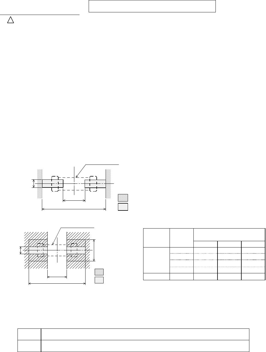
10-5. Attention regarding P.C.B. bending
The following shall be considered when designing and laying out P.C.B.'s.
(1) P.C.B. shall be designed so that products are not subjected to the mechanical stress for board warpage.
<Products direction>
Products shall be located in the sideways
direction (Length:ab) to the mechanical
stress.
(2) Products location on P.C.B. separation.
Products (A, B, C, D) shall be located carefully
so that products are not subject to the
mechanical stress due to warping the board.
Because they may be subjected the mechanical
stress in order of A
CB D.
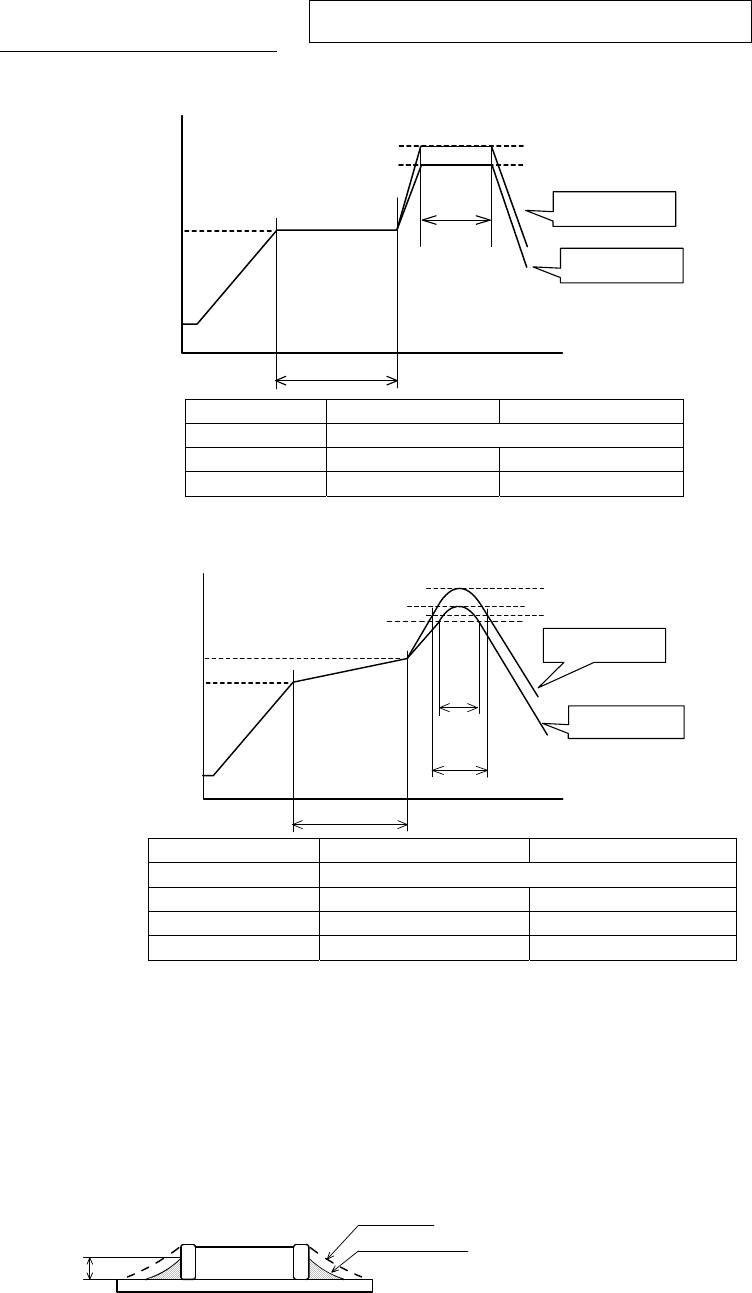
10-6. Mounting density
Add special attention to radiating heat of products when mounting the inductor near the products with heating.
The excessive heat by other products may cause deterioration at joint of this product with substrate.
10-7. Operating Environment
Do not use this product under the following environmental conditions, on deterioration of the Insulation
Resistance of the Ferrite material and/or corrosion of Inner Electrode may result from the use.
(1) in the corrodible atmosphere (acidic gases, alkaline gases, chlorine, sulfur gases, organic gases and etc.)
(2) in the atmosphere where liquid such as organic solvent, may splash on the products.
(3) in the atmosphere where the temperature / humidity changes rapidly and it is easy to dew.
10-8. Resin coating
The impedance value may change and/or it may affect on the product's performance due to high cure-stress of resin
to be used for coating / molding products. So please pay your careful attention when you select resin. In prior to use,
please make the reliability evaluation with the product mounted in your application set.
10-9. Cleaning Conditions
Products shall be cleaned on the following conditions.
(1) Cleaning temperature shall be limited to 60°C max. (40°C max. for IPA.)
(2) Ultrasonic cleaning shall comply with the following conditions, avoiding the resonance phenomenon
at the mounted products and P.C.B.
Power:20W/ max. Frequency:28kHz to 40kHz Time:5 min max.
(3) Cleaner
1.Alternative cleaner
Isopropyl alcohol (IPA)
2.Aqueous agent
PINE ALPHA ST-100S
(4) There shall be no residual flux and residual cleaner after cleaning.
In the case of using aqueous agent, products shall be dried completely after rinse with de-ionized water
in order to remove the cleaner.
(5) Other cleaning
Please contact us.
Poor example
Good example
b
a
Seam
Slit
A
D
B
C
b
a
Length:a
b
Total page

BLM21AG601SN1D

Mfr. #:
Manufacturer:
Description:
EMI Filter Beads, Chips & Arrays 0805 600 OHM
Lifecycle:
New from this manufacturer.
Delivery:
DHL FedEx Ups TNT EMS
Payment:
T/T Paypal Visa MoneyGram Western Union