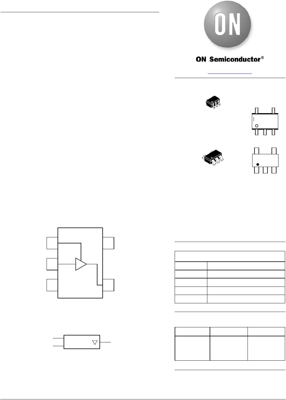
NLVVHC1G126DFT1G

© Semiconductor Components Industries, LLC, 2016
December, 2016 − Rev. 18
1 Publication Order Number:
MC74VHC1G126/D
MC74VHC1G126
Noninverting 3-State Buffer
The MC74VHC1G126 is an advanced high speed CMOS
noninverting 3−state buffer fabricated with silicon gate CMOS
technology. It achieves high speed operation similar to equivalent
Bipolar Schottky TTL while maintaining CMOS low power
dissipation.
The internal circuit is composed of three stages, including a buffered
3−state output which provides high noise immunity and stable output.
The MC74VHC1G126 input structure provides protection when
voltages up to 7 V are applied, regardless of the supply voltage. This
allows the MC74VHC1G126 to be used to interface 5 V circuits to 3 V
circuits.
Features
High Speed: t
PD
= 3.5 ns (Typ) at V
CC
= 5 V
Low Power Dissipation: I
CC
= 1 mA (Max) at T
A
= 25°C
Power Down Protection Provided on Inputs
Balanced Propagation Delays
Pin and Function Compatible with Other Standard Logic Families
Chip Complexity: FETs = 58; Equivalent Gates = 15
NLV Prefix for Automotive and Other Applications Requiring
Unique Site and Control Change Requirements; AEC−Q100
Qualified and PPAP Capable
These Devices are Pb−Free and are RoHS Compliant
Figure 1. Pinout (Top View)
V
CC
OE
IN A
OUT Y
GND
IN A
OUT Y
EN
OE
Figure 2. Logic Symbol
1
2
3
5
4
See detailed ordering and shipping information in the
package dimensions section on page 4 of this data sheet.
ORDERING INFORMATION
FUNCTION TABLE
L
H
X
A Input Y Output
L
H
Z
OE Input
H
H
L
PIN ASSIGNMENT
1
2
3 GND
OE
IN A
4
5V
CC
OUT Y
www.onsemi.com
SC−88A / SOT−353 / SC−70
DF SUFFIX
CASE 419A
TSOP−5 / SOT−23 / SC−59
DT SUFFIX
CASE 483
MARKING
DIAGRAMS
1
5
1
5
1
5
W2 M G
G
W2 = Device Code
M = Date Code*
G = Pb−Free Package
1
5
W2 M G
G
M
(Note: Microdot may be in either location)
*Date Code orientation and/or position may vary
depending upon manufacturing location.
MC74VHC1G126
www.onsemi.com
2
MAXIMUM RATINGS
Symbol Characteristics Value Unit
V
CC
DC Supply Voltage −0.5 to +7.0 V
V
IN
DC Input Voltage −0.5 to +7.0 V
V
OUT
DC Output Voltage V
CC
= 0
High or Low State
−0.5 to 7.0
−0.5 to V
CC
+ 0.5
V
I
IK
Input Diode Current −20 mA
I
OK
Output Diode Current V
OUT
< GND; V
OUT
> V
CC
+20 mA
I
OUT
DC Output Current, per Pin +25 mA
I
CC
DC Supply Current, V
CC
and GND +50 mA
P
D
Power dissipation in still air SC−88A, TSOP−5 200 mW
q
JA
Thermal resistance SC−88A, TSOP−5 333 °C/W
T
L
Lead temperature, 1 mm from case for 10 secs 260 °C
T
J
Junction temperature under bias +150 °C
T
stg
Storage temperature −65 to +150 °C
V
ESD
ESD Withstand Voltage Human Body Model (Note 1)
Machine Model (Note 2)
Charged Device Model (Note 3)
> 2000
> 200
N/A
V
I
Latchup
Latchup Performance Above V
CC
and Below GND at 125°C (Note 4) ±500 mA
Stresses exceeding those listed in the Maximum Ratings table may damage the device. If any of these limits are exceeded, device functionality
should not be assumed, damage may occur and reliability may be affected.
1. Tested to EIA/JESD22−A114−A
2. Tested to EIA/JESD22−A115−A
3. Tested to JESD22−C101−A
4. Tested to EIA/JESD78
RECOMMENDED OPERATING CONDITIONS
Symbol Characteristics Min Max Unit
V
CC
DC Supply Voltage 2.0 5.5 V
V
IN
DC Input Voltage 0.0 5.5 V
V
OUT
DC Output Voltage 0.0 V
CC
V
T
A
Operating Temperature Range −55 +125 °C
t
r
, t
f
Input Rise and Fall Time V
CC
= 3.3 V ± 0.3 V
V
CC
= 5.0 V ± 0.5 V
0
0
100
20
ns/V
Functional operation above the stresses listed in the Recommended Operating Ranges is not implied. Extended exposure to stresses beyond
the Recommended Operating Ranges limits may affect device reliability.
Device Junction Temperature versus
Time to 0.1% Bond Failures
Junction
Temperature °C
Time, Hours Time, Years
80 1,032,200 117.8
90 419,300 47.9
100 178,700 20.4
110 79,600 9.4
120 37,000 4.2
130 17,800 2.0
140 8,900 1.0
1
1 10 100
1000
TIME, YEARS
NORMALIZED FAILURE RATE
T
J
= 80
C°
T
J
= 90
C°
T
J
= 100 C°
T
J
= 110 C°
T
J
= 130 C°
T
J
= 120 C°
FAILURE RATE OF PLASTIC = CERAMIC
UNTIL INTERMETALLICS OCCUR
Figure 3. Failure Rate vs. Time Junction Temperature
MC74VHC1G126
www.onsemi.com
3
DC ELECTRICAL CHARACTERISTICS
Symbo
l
Parameter Test Conditions
V
CC
(V)
T
A
= 25°C T
A
85°C −55 T
A
125°C
Unit
Min Typ Max Min Max Min Max
V
IH
Minimum High−Level
Input Voltage
2.0
3.0
4.5
5.5
1.5
2.1
3.15
3.85
1.5
2.1
3.15
3.85
1.5
2.1
3.15
3.85
V
V
IL
Maximum Low−Level
Input Voltage
2.0
3.0
4.5
5.5
0.5
0.9
1.35
1.65
0.5
0.9
1.35
1.65
0.5
0.9
1.35
1.65
V
V
OH
Minimum High−Level
Output Voltage
V
IN
= V
IH
or V
IL
V
IN
= V
IH
or V
IL
I
OH
= −50 mA
2.0
3.0
4.5
1.9
2.9
4.4
2.0
3.0
4.5
1.9
2.9
4.4
1.9
2.9
4.4
V
V
IN
= V
IH
or V
IL
I
OH
= −4 mA
I
OH
= −8 mA
3.0
4.5
2.58
3.94
2.48
3.80
2.34
3.66
V
V
OL
Maximum Low−Level
Output Voltage
V
IN
= V
IH
or V
IL
V
IN
= V
IH
or V
IL
I
OL
= 50 mA
2.0
3.0
4.5
0.0
0.0
0.0
0.1
0.1
0.1
0.1
0.1
0.1
0.1
0.1
0.1
V
V
IN
= V
IH
or V
IL
I
OL
= 4 mA
I
OL
= 8 mA
3.0
4.5
0.36
0.36
0.44
0.44
0.52
0.52
V
I
OZ
Maximum 3−State
Leakage Current
V
IN
= V
IH
or V
IL
V
OUT
= V
CC
or GND
5.5 ±0.2
5
±2.5 ±2.5
mA
I
IN
Maximum Input
Leakage Current
V
IN
= 5.5 V or GND 0 to
5.5
±0.1 ±1.0 ±1.0
mA
I
CC
Maximum Quiescent
Supply Current
V
IN
= V
CC
or GND 5.5 1.0 20 40
mA
Product parametric performance is indicated in the Electrical Characteristics for the listed test conditions, unless otherwise noted. Product
performance may not be indicated by the Electrical Characteristics if operated under different conditions.
AC ELECTRICAL CHARACTERISTICS C
load
= 50 pF, Input t
r
= t
f
= 3.0 ns
Symbo
l
Parameter Test Conditions
T
A
= 25°C T
A
85°C −55 T
A
125°C
Unit
Min Typ Max Min Max Min Max
t
PLH
,
t
PHL
Maximum Propagation
Delay, Input A to Y
(Figures 3. and 5.)
V
CC
= 3.3 ± 0.3 V C
L
= 15 pF
C
L
= 50 pF
4.5
6.4
8.0
11.5
9.5
13.0
12.0
16.0
ns
V
CC
= 5.0 ± 0.5 V C
L
= 15 pF
C
L
= 50 pF
3.5
4.5
5.5
7.5
6.5
8.5
8.5
10.5
t
PZL
,
t
PZH
Maximum Output Enable
Time, Input OE to Y
(Figures 4. and 5.)
V
CC
= 3.3 ± 0.3 V C
L
= 15 pF
R
L
= 1000 W C
L
= 50 pF
4.5
6.4
8.0
11.5
9.5
13.0
11.5
15.0
ns
V
CC
= 5.0 ± 0.5 V C
L
= 15 pF
R
L
= 1000 W C
L
= 50 pF
3.5
4.5
5.1
7.1
6.0
8.0
8.5
10.5
t
PLZ
,
t
PHZ
Maximum Output Disable
Time, Input OE to Y
(Figures 4. and 5.)
V
CC
= 3.3 ± 0.3 V C
L
= 15 pF
R
L
= 1000 W C
L
= 50 pF
6.5
8.0
9.7
13.2
11.5
15.0
14.5
18.0
ns
V
CC
= 5.0 ± 0.5 V C
L
= 15 pF
R
L
= 1000 W C
L
= 50 pF
4.8
7.0
6.8
8.8
8.0
10.0
10.0
12.0
C
IN
Maximum Input
Capacitance
4.0 10 10 10 pF
C
OUT
Maximum 3−State Output
Capacitance (Output in
High Impedance State)
6.0 pF
C
PD
Power Dissipation Capacitance (Note 5)
Typical @ 25°C, V
CC
= 5.0 V
pF
8.0
5. C
PD
is defined as the value of the internal equivalent capacitance which is calculated from the operating current consumption without load.
Average operating current can be obtained by the equation: I
CC(OPR
)
= C
PD
V
CC
f
in
+ I
CC
. C
PD
is used to determine the no−load dynamic
power consumption; P
D
= C
PD
V
CC
2
f
in
+ I
CC
V
CC
.

NLVVHC1G126DFT1G

Mfr. #:
Manufacturer:
ON Semiconductor
Description:
Buffers & Line Drivers LOG CMOS GATE NOR SNGL
Lifecycle:
New from this manufacturer.
Delivery:
DHL FedEx Ups TNT EMS
Payment:
T/T Paypal Visa MoneyGram Western Union