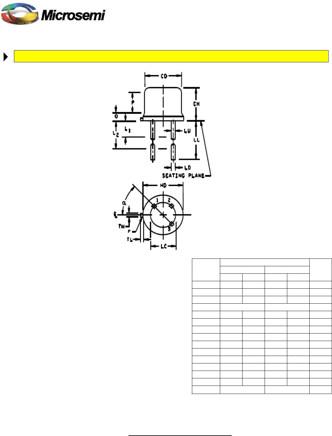
TECHNICAL DATA SHEET
6 Lake Street, Lawrence, MA 01841
1-800-446-1158 / (978) 620-2600 / Fax: (978) 689-0803
Website: http: //www.microsemi.com
T4-LDS-0059 Rev. 2 (100247) Page 2 of 6
ELECTRICAL CHARACTERISTICS (T
A
= +25°C, unless otherwise noted)
Parameters / Test Conditions Symbol Min. Max. Unit
ON CHARACTERISTICS
(4)
Forward-Current Transfer Ratio
I
C
= 0.1mAdc, V
CE
= 10Vdc 2N2906A, L, UA, UB, UBC
2N2907A, L, UA, UB, UBC
40
75
I
C
= 1.0mAdc, V
CE
= 10Vdc 2N2906A, L, UA, UB, UBC
2N2907A, L, UA, UB, UBC
40
100
175
450
I
C
= 10mAdc, V
CE
= 10Vdc 2N2906A, L, UA, UB, UBC
2N2907A, L, UA, UB, UBC
40
100
I
C
= 150mAdc, V
CE
= 10Vdc 2N2906A, L, UA, UB, UBC
2N2907A, L, UA, UB, UBC
40
100
120
300
I
C
= 500mAdc, V
CE
= 10Vdc 2N2906A, L, UA, UB, UBC
2N2907A, L, UA, UB, UBC
h
FE
40
50
Collector-Emitter Saturation Voltage
I
C
= 150mAdc, I
B
= 15mAdc
I
C
= 500mAdc, I
B
= 50mAdc
V
CE(sat)
0.4
1.6
Vdc
Base-Emitter Saturation Voltage
I
C
= 150mAdc, I
B
= 15mAdc
I
C
= 500mAdc, I
B
= 50mAdc
V
BE(sat)
0.6
1.3
2.6
Vdc
DYNAMIC CHARACTERISTICS
Parameters / Test Conditions Symbol Min. Max. Unit
Forward Current Transfer Ratio
I
C
= 1.0mAdc, V
CE
= 10Vdc, f = 1.0kHz 2N2906A, L, UA, UB, UBC
2N2907A, L, UA, UB, UBC
h
fe
40
100
Magnitude of Small–Signal Forward Current Transfer Ratio
I
C
= 20mAdc, V
CE
= 20Vdc, f = 100MHz
|h
fe
|
2.0
Output Capacitance
V
CB
= 10Vdc, I
E
= 0, 100kHz ≤ f ≤ 1.0MHz
C
obo
8.0 pF
Input Capacitance
V
EB
= 2.0Vdc, I
C
= 0, 100kHz ≤ f ≤ 1.0MHz
C
ibo
30 pF
SWITCHING CHARACTERISTICS
Parameters / Test Conditions Symbol Min. Max. Unit
Turn-On Time
V
CC
= 30Vdc; I
C
= 150mAdc; I
B1
= 50mAdc
t
on
45
ηs
Turn-Off Time
V
CC
= 30Vdc; I
C
= 150mAdc; I
B1
= -I
B2
= 50mAdc
t
off
300
ηs
(4) Pulse Test: Pulse Width = 300μs, Duty Cycle ≤ 2.0%.